For a three state TTL following statements are given : (a) It allows to connect outputs directly. (b) It allows to connect the inputs directly. (c) It is used to decrease the switching time. (d) It is used to increase the switching time in order to interface the peripherals for matching the speed with computer. Which of the above are correct ?
(a) and (c)
To determine the correct statements regarding a three-state TTL (Transistor-Transistor Logic), let's analyze each statement:
- (a) It allows to connect outputs directly.
- This is correct. The three-state logic allows multiple outputs to be connected to a common bus line because it can effectively "disconnect" its output by setting it to a high-impedance (Hi-Z) state. This feature is critical for bus systems where multiple logic circuits share the same line, and at any given time, only one should drive the line actively.
- (b) It allows to connect the inputs directly.
- This statement is incorrect. Three-state logic primarily affects outputs rather than inputs. While inputs can be connected directly in digital logic, this isn't a unique feature or result of three-state logic.
- (c) It is used to decrease the switching time.
- This is correct. While technically three-state logic itself does not directly decrease the switching time, it simplifies the connection of multiple outputs, thereby, in practice, streamlining processes in a circuit which can decrease perceived switching times in complex circuits.
- (d) It is used to increase the switching time in order to interface the peripherals for matching the speed with computer.
- This is incorrect. The three-state logic is not used to increase the switching time. Instead, it facilitates better control and coordination in digital systems but does not inherently increase switching times for speed matching purposes.
Therefore, the correct statements about a three-state TTL are (a) and (c).
Similar Questions
Arrange in ascending order based on power dissipation the following logic families :
(i) ECL
(ii) TTL
(iii) CMOSMatch the following :
List – I List – II a. I2L i. XOR b. high impedance state ii. non-saturation logic c. controlled inverter iii. tristate d. ECL iv. bipolar logic Codes :
The logic families have fan out more than TTL
A. RTL
B. ECL
C. DTL
D. CMOS
Choose the correct answer from the options given below.
Match the following lists in terms of power dissipation/Gate:
List – I List – II a. BiCMOS i. 6 mW b. ECL ii. 2.75 μW c. CMOS (AHC) iii. 25 mW to 73 mW d. bipolar TTL (F) iv. 17 μw Choose the correct answer from the codes given below:
Arrange the following in terms of decreasing order of power dissipation :
(a) CMOS
(b) ECL
(c) TTL
(d) MOS
The correct sequence of decreasing order of power dissipation is
Match the following in context of Fan out of various families :
List - I List - II (a) DTL (i) 20 (b) TTL (ii) 30 (c) PMOS (iii) 50 (d) CMOS (iv) 5 to 15 Codes :
For wired AND connection we should use :
Match the following :
List - I List - II (a) TTL (i) Consumer maximum power (b) ECL (ii) Highest Packaging Density (c) NMOS (iii) Least power consumption (d) CMOS (iv) Saturated logic Codes :
Match the following lists :
List – I List – II a. IC 7400 i. Quad 2-input NOR gate b. IC 7402 ii. Quad 2-input AND gate c. IC 7408 iii. Quad 2-input OR gate d. IC 7432 iv. Quad 2-input NAND gate Given that for a logic family :
(A) VOH is the maximum output high level voltage
(B) VOL is the maximum input low level voltage
(C) VIH is the minimum input acceptable input high voltage level
(D) VIL is the minimum acceptable input low voltage levelChoose the most appropriate answer from the options given below :
Important Questions from Logic Families
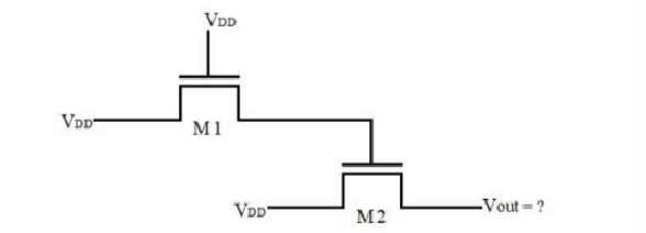
What is the voltage at the output node of the given circuit? Assume $V_{DD} = 1.8V$ and threshold voltage of the transistor $V_{TN} = 0.4V$ and body bias effect is negligible.
Arrange in ascending order based on power dissipation the following logic families :
(i) ECL
(ii) TTL
(iii) CMOSMatch the following :
List – I List – II a. I2L i. XOR b. high impedance state ii. non-saturation logic c. controlled inverter iii. tristate d. ECL iv. bipolar logic Codes :
The logic families have fan out more than TTL
A. RTL
B. ECL
C. DTL
D. CMOS
Choose the correct answer from the options given below.
Match the following lists in terms of power dissipation/Gate:
List – I List – II a. BiCMOS i. 6 mW b. ECL ii. 2.75 μW c. CMOS (AHC) iii. 25 mW to 73 mW d. bipolar TTL (F) iv. 17 μw Choose the correct answer from the codes given below: