
In an FET, following characteristics are given : 1. JFET is called as variable current resistor. Which one of the following is true ?
2. JFET is called Voltage variable resistor.
3. \(g_{d}=g_{d0}\left(1-\dfrac{V_{GS}}{V_{P}}\right)\), where gd0 is value of drain to source conductance for zero bias.
4. \(g_{d}=g_{d0}\left(1+\dfrac{V_{GS}}{V_{P}}\right)^{2}\)
2 and 3
Statements 2 and 3 are the true pair — option 4.
Statement 2 — the name. Below pinch-off, in the ohmic or triode region, the JFET's drain-source path behaves as a resistance whose value is set by the gate voltage. Since the gate junction is reverse biased it draws essentially no current, the control is by voltage alone, and the device is universally called a voltage variable resistor or voltage-controlled resistor. Statement 1's "variable current resistor" inverts this: the JFET is a voltage-controlled device, unlike the BJT, whose collector current is set by base current.
Statement 3 — the conductance law. Channel conductance falls as the gate reverse bias widens the depletion regions and squeezes the conducting channel. Taking the linear form given,
\(g_{d}=g_{d0}\left(1-\dfrac{V_{GS}}{V_{P}}\right)\)
the limits behave correctly: at \(V_{GS}=0\) it returns \(g_{d}=g_{d0}\), the zero-bias value, and at \(V_{GS}=V_{P}\) it gives \(g_{d}=0\) — the channel pinched off and the resistance infinite. Both end points are right.
Statement 4 fails at both ends. With a plus sign, \(V_{GS}=V_{P}\) gives \(g_{d}=4g_{d0}\) — conductance quadrupled at pinch-off, the exact opposite of what happens. The squared form belongs to a different relation altogether, the drain-current equation in saturation:
\(I_{D}=I_{DSS}\left(1-\dfrac{V_{GS}}{V_{P}}\right)^{2}\)
The distractor is built by borrowing that square-law exponent and flipping the sign.
| Statement | Verdict |
|---|---|
| 1. Variable current resistor | ✗ The JFET is voltage controlled |
| 2. Voltage variable resistor | ✓ |
| 3. gd with the minus sign | ✓ Correct at both limits |
| 4. Squared, with a plus sign | ✗ Predicts more conductance at pinch-off |
The practical use of the ohmic region is exactly what statement 2 names: JFETs serve as electronically variable attenuators in automatic gain control, as the gain-setting element in Wien-bridge oscillators, and as analogue switches — the drain-source resistance running from a few hundred ohms when on to many megohms when off.
Hence, statements 2 and 3 are true.
Similar Questions
For MOSFET, consider the following statements
A. In triode region, FET works as voltage variable resistor
B. For p-channel MOSFET, if VSG \(\gt\) |VTp|, then transistor will be in off mode
C. Amplification factor is inversly proportional to the value of VGS/Vp.
D. In saturation region, FET is used as amplifier.
E. For depletion MOSFET, channel is diffused and current flows even if VGS is zero
Choose the correct answer from the options given below :
Transfer characteristics for n-channel FET as a function of temperature T is shown in the figure
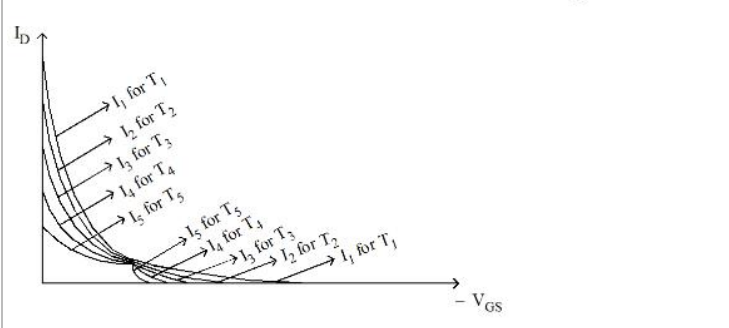
Choose the correct answer from the options given below :
When gate to source voltage of a FET changes from –5.2 volt to –5 volts, the corresponding drain current changes from 1 mA to 1.3 mA, the transconductance is
In a JFET the gate to source voltage is given as
In a JFET self-bias configuration shown below :
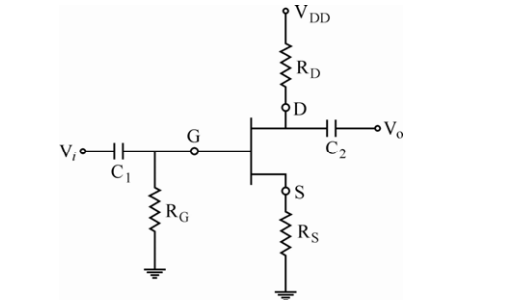
The drain current is
(a) \(K\dfrac{W}{L}(V_{gs}-V_{th})V_{ds}\)
(b) \(I_{DSS}\left(1-\dfrac{I_DR_S}{V_P}\right)^{2}\)
(c) \(I_{DSS}\left(1+\dfrac{I_DR_S}{V_P}\right)^{2}\)
(d) \(K\dfrac{W}{L}(V_{gs}-V_{th})^{2}\)
Out of these which are correct ?
Assertion (A) : FET is a device, which depends for its operation on the control of field or voltage due to applied current.
Reason (R) : FET has a very high input resistance of the order of mega-ohms. It is also immune to radiations.
Match the following :
List - I List - II (circuit in the original question) (a) JFET VGS = 0V (i) 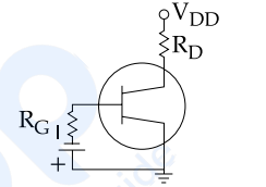
(b) JFET self-bias (ii) 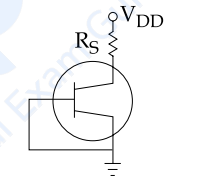
(c) JFET Fixed bias (iii) 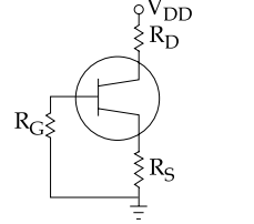
(d) FET Low Frequencies circuit (iv) 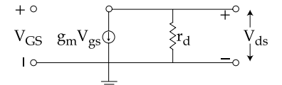
Codes :
Which of the following statements are valid for JFET ?
(a) \(I_{DS}=I_{DSS}\left(1-\dfrac{V_{GS}}{V_P}\right)\)
(b) \(I_{DS}=I_{DSS}\left(1+\dfrac{V_{GS}}{V_P}\right)\)
(c) \(\mu=\dfrac{g_m}{r_d}\)
(d) \(\mu=g_m\cdot r_d\)
Options :
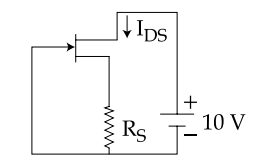
The JFET in a circuit shown in Figure, has an IDSS = 10 mA and Vp = − 5V. The value of resistance RS for a drain current IDS = 6.4 mA is (Choose the nearest value)
In a certain FET circuit, VGS = 0V, VDD = 15V, IDSS = 15 mA, and RD = 470Ω. If RD is decreased to 330 Ω, IDSS is :
Important Questions from Field Effect Transistors
Which of the following is the characteristic of Field-effect transistor?
- In junction field effect transistor, the drain current can be approximated as:
The expression for the transconductance (g m) of a JFET is:
Field Effect transistor is:
The main drawback of a JFET is its



