
In a JFET self-bias configuration shown below : The drain current is (a) \(K\dfrac{W}{L}(V_{gs}-V_{th})V_{ds}\) (b) \(I_{DSS}\left(1-\dfrac{I_DR_S}{V_P}\right)^{2}\) (c) \(I_{DSS}\left(1+\dfrac{I_DR_S}{V_P}\right)^{2}\) (d) \(K\dfrac{W}{L}(V_{gs}-V_{th})^{2}\) Out of these which are correct ?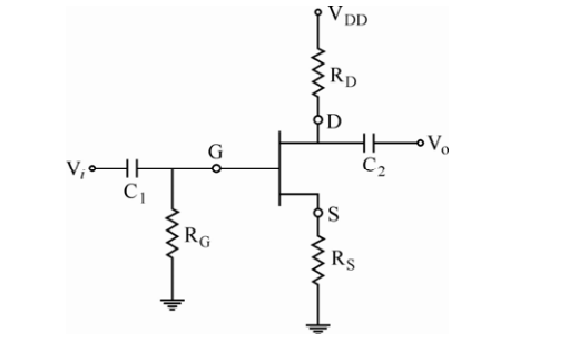
(b) is wrong but (c) is correct.
How self-bias works. No separate gate supply is used. The drain current flowing through RS raises the source above ground, while RG holds the gate at 0 V (no gate current flows). The gate is therefore negative with respect to the source:
\(V_{GS}=V_G-V_S=0-I_DR_S=-I_DR_S\)
This self-adjusting bias is why the configuration is stable: if ID tries to rise, VGS becomes more negative and pushes it back down.
Substitute into Shockley's equation.
\(I_D=I_{DSS}\left(1-\dfrac{V_{GS}}{V_P}\right)^{2}\)
\(I_D=I_{DSS}\left(1-\dfrac{-I_DR_S}{V_P}\right)^{2}=I_{DSS}\left(1+\dfrac{I_DR_S}{V_P}\right)^{2}\)
The double negative turns the minus into a plus, so statement (c) is the correct self-bias equation and (b), with the minus sign retained, is wrong. That is precisely what option 3 states.
Why (a) and (d) are irrelevant here. Both are written with K, W/L and Vth — the parameters of a MOSFET. A JFET is described by IDSS and the pinch-off voltage VP, and it has no threshold voltage or oxide to give a W/L conduction parameter. Spotting the wrong device model immediately removes half the statements. (Expression (a) is additionally the triode-region form, not a saturation current.)
How the equation is used. It is implicit — ID appears on both sides — so in practice one either solves the resulting quadratic or finds the operating point graphically, by drawing the bias line \(V_{GS}=-I_DR_S\) across the transfer characteristic and reading off the intersection.
Hence, the correct choice is (b) is wrong but (c) is correct.
Similar Questions
In an FET, following characteristics are given :
1. JFET is called as variable current resistor.
2. JFET is called Voltage variable resistor.
3. \(g_{d}=g_{d0}\left(1-\dfrac{V_{GS}}{V_{P}}\right)\), where gd0 is value of drain to source conductance for zero bias.
4. \(g_{d}=g_{d0}\left(1+\dfrac{V_{GS}}{V_{P}}\right)^{2}\)Which one of the following is true ?
For MOSFET, consider the following statements
A. In triode region, FET works as voltage variable resistor
B. For p-channel MOSFET, if VSG \(\gt\) |VTp|, then transistor will be in off mode
C. Amplification factor is inversly proportional to the value of VGS/Vp.
D. In saturation region, FET is used as amplifier.
E. For depletion MOSFET, channel is diffused and current flows even if VGS is zero
Choose the correct answer from the options given below :
Transfer characteristics for n-channel FET as a function of temperature T is shown in the figure
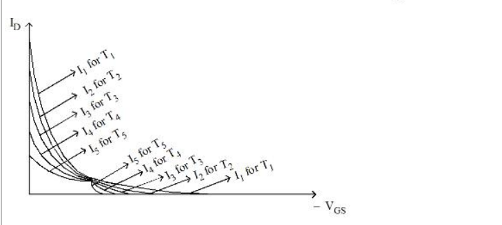
Choose the correct answer from the options given below :
When gate to source voltage of a FET changes from –5.2 volt to –5 volts, the corresponding drain current changes from 1 mA to 1.3 mA, the transconductance is
In a JFET the gate to source voltage is given as
Assertion (A) : FET is a device, which depends for its operation on the control of field or voltage due to applied current.
Reason (R) : FET has a very high input resistance of the order of mega-ohms. It is also immune to radiations.
Match the following :
List - I List - II (circuit in the original question) (a) JFET VGS = 0V (i) 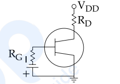
(b) JFET self-bias (ii) 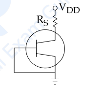
(c) JFET Fixed bias (iii) 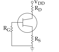
(d) FET Low Frequencies circuit (iv) 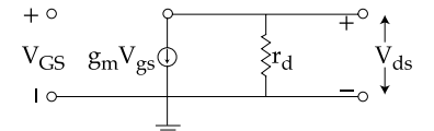
Codes :
Which of the following statements are valid for JFET ?
(a) \(I_{DS}=I_{DSS}\left(1-\dfrac{V_{GS}}{V_P}\right)\)
(b) \(I_{DS}=I_{DSS}\left(1+\dfrac{V_{GS}}{V_P}\right)\)
(c) \(\mu=\dfrac{g_m}{r_d}\)
(d) \(\mu=g_m\cdot r_d\)
Options :
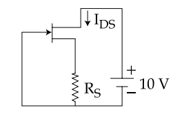
The JFET in a circuit shown in Figure, has an IDSS = 10 mA and Vp = − 5V. The value of resistance RS for a drain current IDS = 6.4 mA is (Choose the nearest value)
In a certain FET circuit, VGS = 0V, VDD = 15V, IDSS = 15 mA, and RD = 470Ω. If RD is decreased to 330 Ω, IDSS is :
Important Questions from Field Effect Transistors
Which of the following is the characteristic of Field-effect transistor?
- In junction field effect transistor, the drain current can be approximated as:
The expression for the transconductance (g m) of a JFET is:
Field Effect transistor is:
The main drawback of a JFET is its



