
Transfer characteristics for n-channel FET as a function of temperature T is shown in the figure Choose the correct answer from the options given below :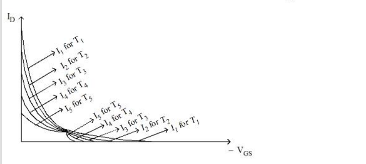
\(T_1 \lt T_2 \lt T_3 \lt T_4 \lt T_5\)
What the figure shows. Drain current ID is plotted against gate bias for an n-channel FET, one curve per temperature — curve I1 for T1 through I5 for T5. The curve carrying the largest drain current is I1, and the current falls progressively down to I5.
The physics that links current to temperature. Two competing effects act on a FET as temperature rises:
1. The carrier mobility falls, because lattice (phonon) scattering increases: roughly \(\mu \propto T^{-3/2}\). Since \(I_D \propto \mu\), this reduces the drain current.
2. The threshold (pinch-off) voltage magnitude falls by about 2–3 mV/°C, which by itself would increase the current.
Over most of the transfer characteristic the mobility term dominates, so higher temperature means lower drain current at a given gate voltage. (The two effects cancel at one particular bias — the zero-temperature-coefficient point — which is exploited to make bias-stable amplifier stages, and it is why the curves in such a figure all pass close to a common crossover point.)
Apply it to the curves. Largest current ⇒ lowest temperature, so I1 (topmost) corresponds to the coolest device and I5 (lowest) to the hottest:
\(T_1 \lt T_2 \lt T_3 \lt T_4 \lt T_5\)
Why the other options are impossible. Option 1 reverses the physics — it would require current to rise with temperature over the whole characteristic. Options 3 and 4 claim all five temperatures are equal (0 K or room temperature), which cannot produce five distinct curves at all; and at 0 K a semiconductor would have no thermally generated carriers.
Practical consequence. Because ID falls as the device heats, a FET has a built-in negative feedback against thermal runaway — a hot spot conducts less current — which is why power MOSFETs can safely be paralleled, whereas BJTs (whose current rises with temperature) need emitter ballast resistors.
Hence, the correct ordering is \(T_1 \lt T_2 \lt T_3 \lt T_4 \lt T_5\).
Similar Questions
In an FET, following characteristics are given :
1. JFET is called as variable current resistor.
2. JFET is called Voltage variable resistor.
3. \(g_{d}=g_{d0}\left(1-\dfrac{V_{GS}}{V_{P}}\right)\), where gd0 is value of drain to source conductance for zero bias.
4. \(g_{d}=g_{d0}\left(1+\dfrac{V_{GS}}{V_{P}}\right)^{2}\)Which one of the following is true ?
For MOSFET, consider the following statements
A. In triode region, FET works as voltage variable resistor
B. For p-channel MOSFET, if VSG \(\gt\) |VTp|, then transistor will be in off mode
C. Amplification factor is inversly proportional to the value of VGS/Vp.
D. In saturation region, FET is used as amplifier.
E. For depletion MOSFET, channel is diffused and current flows even if VGS is zero
Choose the correct answer from the options given below :
When gate to source voltage of a FET changes from –5.2 volt to –5 volts, the corresponding drain current changes from 1 mA to 1.3 mA, the transconductance is
In a JFET the gate to source voltage is given as
In a JFET self-bias configuration shown below :
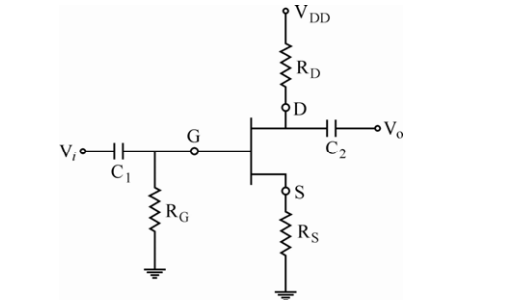
The drain current is
(a) \(K\dfrac{W}{L}(V_{gs}-V_{th})V_{ds}\)
(b) \(I_{DSS}\left(1-\dfrac{I_DR_S}{V_P}\right)^{2}\)
(c) \(I_{DSS}\left(1+\dfrac{I_DR_S}{V_P}\right)^{2}\)
(d) \(K\dfrac{W}{L}(V_{gs}-V_{th})^{2}\)
Out of these which are correct ?
Assertion (A) : FET is a device, which depends for its operation on the control of field or voltage due to applied current.
Reason (R) : FET has a very high input resistance of the order of mega-ohms. It is also immune to radiations.
Match the following :
List - I List - II (circuit in the original question) (a) JFET VGS = 0V (i) 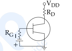
(b) JFET self-bias (ii) 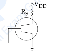
(c) JFET Fixed bias (iii) 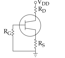
(d) FET Low Frequencies circuit (iv) 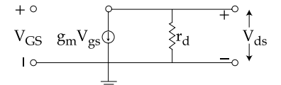
Codes :
Which of the following statements are valid for JFET ?
(a) \(I_{DS}=I_{DSS}\left(1-\dfrac{V_{GS}}{V_P}\right)\)
(b) \(I_{DS}=I_{DSS}\left(1+\dfrac{V_{GS}}{V_P}\right)\)
(c) \(\mu=\dfrac{g_m}{r_d}\)
(d) \(\mu=g_m\cdot r_d\)
Options :
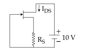
The JFET in a circuit shown in Figure, has an IDSS = 10 mA and Vp = − 5V. The value of resistance RS for a drain current IDS = 6.4 mA is (Choose the nearest value)
In a certain FET circuit, VGS = 0V, VDD = 15V, IDSS = 15 mA, and RD = 470Ω. If RD is decreased to 330 Ω, IDSS is :
Important Questions from Field Effect Transistors
Which of the following is the characteristic of Field-effect transistor?
- In junction field effect transistor, the drain current can be approximated as:
The expression for the transconductance (g m) of a JFET is:
Field Effect transistor is:
The main drawback of a JFET is its



