
In a certain FET circuit, VGS = 0V, VDD = 15V, IDSS = 15 mA, and RD = 470Ω. If RD is decreased to 330 Ω, IDSS is :
15 mA
Read what is being asked: not the drain current, but IDSS. That distinction is the whole question.
IDSS is a device parameter, not a circuit quantity. It is defined as the drain-to-source current with the gate shorted to the source, measured in the saturation region:
\(I_{DSS}=\left.I_{D}\right|_{V_{GS}=0,\ \left|V_{DS}\right|\gt\left|V_{P}\right|}\)
Its value is fixed at manufacture by the channel's doping, length and width. Nothing an external resistor does can alter it, so changing RD from 470 Ω to 330 Ω leaves IDSS at 15 mA — option 3.
Why the circuit values are given at all is to make the distractors plausible, and it is worth seeing what they would mean. With VGS = 0 the device tries to pass its full IDSS, so check whether the circuit can support it:
| RD | Drop if ID = 15 mA | VDS = 15 − drop |
|---|---|---|
| 470 Ω | 7.05 V | 7.95 V |
| 330 Ω | 4.95 V | 10.05 V |
In both cases VDS stays comfortably above a typical pinch-off voltage, so the JFET remains in saturation and the actual drain current is also 15 mA in both cases — reducing RD merely raises VDS. The answer would be 15 mA whichever way the question is read, which is a satisfying cross-check.
The physical reason the current does not rise is that in saturation the FET behaves as a current source, not a resistor. Beyond pinch-off the channel is constricted at the drain end and the drain current becomes almost independent of VDS:
\(I_{D}=I_{DSS}\left(1-\dfrac{V_{GS}}{V_{P}}\right)^{2}\)
which contains no RD and no VDS at all. Only if RD were made so large that VDS fell below \(V_{GS}-V_{P}\) would the device enter the ohmic region and the current start to depend on the external resistor — and reducing RD, as here, moves further away from that boundary.
Option 1 (19.5 mA) is the trap for anyone who reasons that less resistance must mean more current, as it would for a plain resistive circuit. A saturated FET does not obey that intuition, and neither does a BJT in its active region — both are current sources whose output is set by their input, not by their load.
Hence, IDSS remains 15 mA.
Similar Questions
In an FET, following characteristics are given :
1. JFET is called as variable current resistor.
2. JFET is called Voltage variable resistor.
3. \(g_{d}=g_{d0}\left(1-\dfrac{V_{GS}}{V_{P}}\right)\), where gd0 is value of drain to source conductance for zero bias.
4. \(g_{d}=g_{d0}\left(1+\dfrac{V_{GS}}{V_{P}}\right)^{2}\)Which one of the following is true ?
For MOSFET, consider the following statements
A. In triode region, FET works as voltage variable resistor
B. For p-channel MOSFET, if VSG \(\gt\) |VTp|, then transistor will be in off mode
C. Amplification factor is inversly proportional to the value of VGS/Vp.
D. In saturation region, FET is used as amplifier.
E. For depletion MOSFET, channel is diffused and current flows even if VGS is zero
Choose the correct answer from the options given below :
Transfer characteristics for n-channel FET as a function of temperature T is shown in the figure
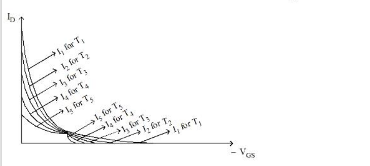
Choose the correct answer from the options given below :
When gate to source voltage of a FET changes from –5.2 volt to –5 volts, the corresponding drain current changes from 1 mA to 1.3 mA, the transconductance is
In a JFET the gate to source voltage is given as
In a JFET self-bias configuration shown below :
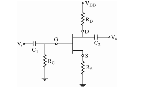
The drain current is
(a) \(K\dfrac{W}{L}(V_{gs}-V_{th})V_{ds}\)
(b) \(I_{DSS}\left(1-\dfrac{I_DR_S}{V_P}\right)^{2}\)
(c) \(I_{DSS}\left(1+\dfrac{I_DR_S}{V_P}\right)^{2}\)
(d) \(K\dfrac{W}{L}(V_{gs}-V_{th})^{2}\)
Out of these which are correct ?
Assertion (A) : FET is a device, which depends for its operation on the control of field or voltage due to applied current.
Reason (R) : FET has a very high input resistance of the order of mega-ohms. It is also immune to radiations.
Match the following :
List - I List - II (circuit in the original question) (a) JFET VGS = 0V (i) 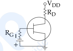
(b) JFET self-bias (ii) 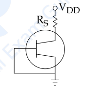
(c) JFET Fixed bias (iii) 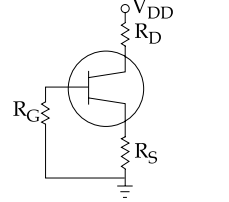
(d) FET Low Frequencies circuit (iv) 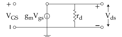
Codes :
Which of the following statements are valid for JFET ?
(a) \(I_{DS}=I_{DSS}\left(1-\dfrac{V_{GS}}{V_P}\right)\)
(b) \(I_{DS}=I_{DSS}\left(1+\dfrac{V_{GS}}{V_P}\right)\)
(c) \(\mu=\dfrac{g_m}{r_d}\)
(d) \(\mu=g_m\cdot r_d\)
Options :
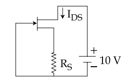
The JFET in a circuit shown in Figure, has an IDSS = 10 mA and Vp = − 5V. The value of resistance RS for a drain current IDS = 6.4 mA is (Choose the nearest value)
Important Questions from Field Effect Transistors
Which of the following is the characteristic of Field-effect transistor?
- In junction field effect transistor, the drain current can be approximated as:
The expression for the transconductance (g m) of a JFET is:
Field Effect transistor is:
The main drawback of a JFET is its



