
Assertion (A) : FET is a device, which depends for its operation on the control of field or voltage due to applied current. Reason (R) : FET has a very high input resistance of the order of mega-ohms. It is also immune to radiations.
(A) is false, but (R) is true.
Assertion — FALSE, and the flaw is in a single phrase. A field-effect transistor is controlled by the voltage applied to its gate, which sets up an electric field that widens or narrows the channel:
\(I_D=f(V_{GS})\)
The assertion says the field is due to an applied current, which inverts the defining property. It is the BJT that is current-controlled (\(I_C=\beta I_B\)); the FET is the voltage-controlled member of the pair, and that is the whole basis of the distinction between them.
Reason — TRUE on both counts.
High input resistance: the gate of a JFET is a reverse-biased junction and the gate of a MOSFET is separated by an insulating oxide, so gate current is only picoamps. Input resistance runs from mega-ohms for a JFET to 1012 Ω or more for a MOSFET — which is exactly why FETs are used at the front end of electrometers, pH meters and instrumentation amplifiers.
Radiation immunity: a FET is a unipolar, majority-carrier device. Radiation damage acts mainly by creating recombination centres that destroy minority-carrier lifetime — which cripples a BJT but barely affects a device whose conduction never depends on minority carriers. Hence FETs are preferred in space and nuclear environments.
Combining: the reason is a correct pair of statements about the FET, but the assertion misdescribes how the device works. A is false while R is true.
Note that if the assertion had read "control of the field due to applied voltage", both statements would be true and R would arguably explain the high input resistance — which is precisely the discrimination this item is testing.
Hence, (A) is false, but (R) is true.
Similar Questions
In an FET, following characteristics are given :
1. JFET is called as variable current resistor.
2. JFET is called Voltage variable resistor.
3. \(g_{d}=g_{d0}\left(1-\dfrac{V_{GS}}{V_{P}}\right)\), where gd0 is value of drain to source conductance for zero bias.
4. \(g_{d}=g_{d0}\left(1+\dfrac{V_{GS}}{V_{P}}\right)^{2}\)Which one of the following is true ?
For MOSFET, consider the following statements
A. In triode region, FET works as voltage variable resistor
B. For p-channel MOSFET, if VSG \(\gt\) |VTp|, then transistor will be in off mode
C. Amplification factor is inversly proportional to the value of VGS/Vp.
D. In saturation region, FET is used as amplifier.
E. For depletion MOSFET, channel is diffused and current flows even if VGS is zero
Choose the correct answer from the options given below :
Transfer characteristics for n-channel FET as a function of temperature T is shown in the figure
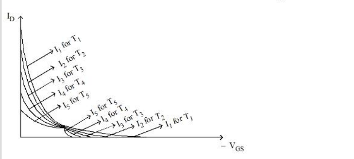
Choose the correct answer from the options given below :
When gate to source voltage of a FET changes from –5.2 volt to –5 volts, the corresponding drain current changes from 1 mA to 1.3 mA, the transconductance is
In a JFET the gate to source voltage is given as
In a JFET self-bias configuration shown below :
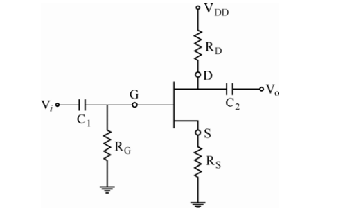
The drain current is
(a) \(K\dfrac{W}{L}(V_{gs}-V_{th})V_{ds}\)
(b) \(I_{DSS}\left(1-\dfrac{I_DR_S}{V_P}\right)^{2}\)
(c) \(I_{DSS}\left(1+\dfrac{I_DR_S}{V_P}\right)^{2}\)
(d) \(K\dfrac{W}{L}(V_{gs}-V_{th})^{2}\)
Out of these which are correct ?
Match the following :
List - I List - II (circuit in the original question) (a) JFET VGS = 0V (i) 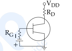
(b) JFET self-bias (ii) 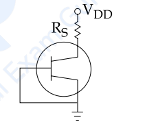
(c) JFET Fixed bias (iii) 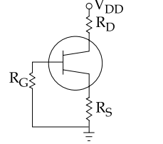
(d) FET Low Frequencies circuit (iv) 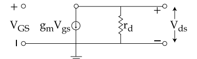
Codes :
Which of the following statements are valid for JFET ?
(a) \(I_{DS}=I_{DSS}\left(1-\dfrac{V_{GS}}{V_P}\right)\)
(b) \(I_{DS}=I_{DSS}\left(1+\dfrac{V_{GS}}{V_P}\right)\)
(c) \(\mu=\dfrac{g_m}{r_d}\)
(d) \(\mu=g_m\cdot r_d\)
Options :
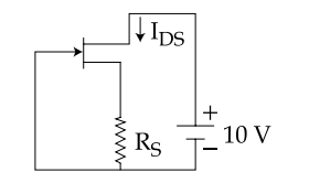
The JFET in a circuit shown in Figure, has an IDSS = 10 mA and Vp = − 5V. The value of resistance RS for a drain current IDS = 6.4 mA is (Choose the nearest value)
In a certain FET circuit, VGS = 0V, VDD = 15V, IDSS = 15 mA, and RD = 470Ω. If RD is decreased to 330 Ω, IDSS is :
Important Questions from Field Effect Transistors
Which of the following is the characteristic of Field-effect transistor?
- In junction field effect transistor, the drain current can be approximated as:
The expression for the transconductance (g m) of a JFET is:
Field Effect transistor is:
The main drawback of a JFET is its



