
In a JFET the gate to source voltage is given as
\(V_p\left(1-\sqrt{\dfrac{I_{ds}}{I_{dss}}}\right)\)
Start from Shockley's equation, which describes a JFET in the saturation (pinch-off) region:
\(I_{ds}=I_{dss}\left(1-\dfrac{V_{gs}}{V_p}\right)^{2}\)
where Idss is the drain current at Vgs = 0 and Vp is the pinch-off (gate cut-off) voltage.
Step 1 — divide through and take the square root.
\(\dfrac{I_{ds}}{I_{dss}}=\left(1-\dfrac{V_{gs}}{V_p}\right)^{2}\)
\(\sqrt{\dfrac{I_{ds}}{I_{dss}}}=1-\dfrac{V_{gs}}{V_p}\)
Step 2 — make Vgs the subject.
\(\dfrac{V_{gs}}{V_p}=1-\sqrt{\dfrac{I_{ds}}{I_{dss}}}\)
\(V_{gs}=V_p\left(1-\sqrt{\dfrac{I_{ds}}{I_{dss}}}\right)\)
which is option 4.
How to eliminate the others by inspection. Two checks settle it without algebra:
The square must disappear. Shockley's law is squared in the current direction, so inverting it must produce a square root, not another square. That rules out options 1 and 2.
The ratio must be Ids/Idss, not its reciprocal. Since \(I_{ds}\le I_{dss}\) the ratio is at most 1, so the bracket runs from 1 (at cut-off, where Ids = 0, giving Vgs = Vp) down to 0 (at Ids = Idss, giving Vgs = 0). Option 3 uses the inverted ratio, which would exceed 1 and give a positive bracket of the wrong size.
Check the two end points in the correct expression: at \(I_{ds}=I_{dss}\) it gives Vgs = 0 ✓, and at \(I_{ds}=0\) it gives Vgs = Vp ✓ — exactly the two anchor points of the transfer curve.
Hence, \(V_{gs}=V_p\left(1-\sqrt{\dfrac{I_{ds}}{I_{dss}}}\right)\).
Similar Questions
In an FET, following characteristics are given :
1. JFET is called as variable current resistor.
2. JFET is called Voltage variable resistor.
3. \(g_{d}=g_{d0}\left(1-\dfrac{V_{GS}}{V_{P}}\right)\), where gd0 is value of drain to source conductance for zero bias.
4. \(g_{d}=g_{d0}\left(1+\dfrac{V_{GS}}{V_{P}}\right)^{2}\)Which one of the following is true ?
For MOSFET, consider the following statements
A. In triode region, FET works as voltage variable resistor
B. For p-channel MOSFET, if VSG \(\gt\) |VTp|, then transistor will be in off mode
C. Amplification factor is inversly proportional to the value of VGS/Vp.
D. In saturation region, FET is used as amplifier.
E. For depletion MOSFET, channel is diffused and current flows even if VGS is zero
Choose the correct answer from the options given below :
Transfer characteristics for n-channel FET as a function of temperature T is shown in the figure
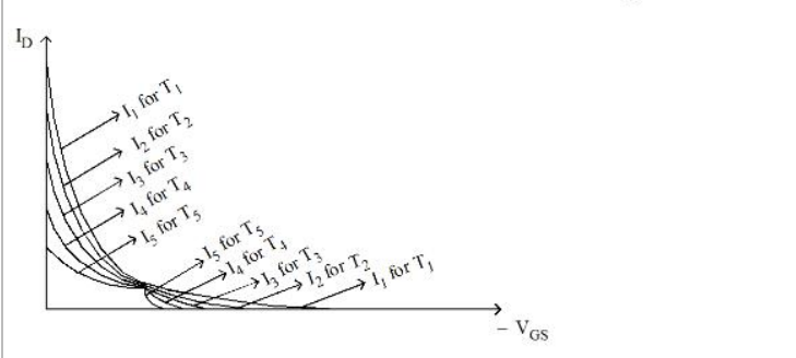
Choose the correct answer from the options given below :
When gate to source voltage of a FET changes from –5.2 volt to –5 volts, the corresponding drain current changes from 1 mA to 1.3 mA, the transconductance is
In a JFET self-bias configuration shown below :
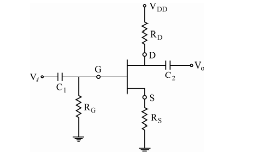
The drain current is
(a) \(K\dfrac{W}{L}(V_{gs}-V_{th})V_{ds}\)
(b) \(I_{DSS}\left(1-\dfrac{I_DR_S}{V_P}\right)^{2}\)
(c) \(I_{DSS}\left(1+\dfrac{I_DR_S}{V_P}\right)^{2}\)
(d) \(K\dfrac{W}{L}(V_{gs}-V_{th})^{2}\)
Out of these which are correct ?
Assertion (A) : FET is a device, which depends for its operation on the control of field or voltage due to applied current.
Reason (R) : FET has a very high input resistance of the order of mega-ohms. It is also immune to radiations.
Match the following :
List - I List - II (circuit in the original question) (a) JFET VGS = 0V (i) 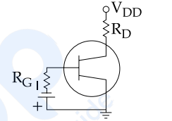
(b) JFET self-bias (ii) 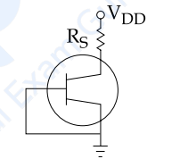
(c) JFET Fixed bias (iii) 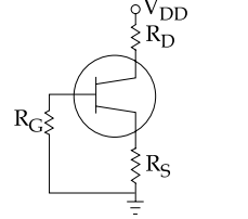
(d) FET Low Frequencies circuit (iv) 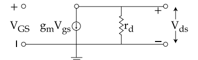
Codes :
Which of the following statements are valid for JFET ?
(a) \(I_{DS}=I_{DSS}\left(1-\dfrac{V_{GS}}{V_P}\right)\)
(b) \(I_{DS}=I_{DSS}\left(1+\dfrac{V_{GS}}{V_P}\right)\)
(c) \(\mu=\dfrac{g_m}{r_d}\)
(d) \(\mu=g_m\cdot r_d\)
Options :
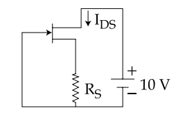
The JFET in a circuit shown in Figure, has an IDSS = 10 mA and Vp = − 5V. The value of resistance RS for a drain current IDS = 6.4 mA is (Choose the nearest value)
In a certain FET circuit, VGS = 0V, VDD = 15V, IDSS = 15 mA, and RD = 470Ω. If RD is decreased to 330 Ω, IDSS is :
Important Questions from Field Effect Transistors
Which of the following is the characteristic of Field-effect transistor?
- In junction field effect transistor, the drain current can be approximated as:
The expression for the transconductance (g m) of a JFET is:
Field Effect transistor is:
The main drawback of a JFET is its



