
Which of the following statements are valid for JFET ? (a) \(I_{DS}=I_{DSS}\left(1-\dfrac{V_{GS}}{V_P}\right)\) (b) \(I_{DS}=I_{DSS}\left(1+\dfrac{V_{GS}}{V_P}\right)\) (c) \(\mu=\dfrac{g_m}{r_d}\) (d) \(\mu=g_m\cdot r_d\) Options :
(a) and (d) are true
This question was cancelled by UGC. The official answer key records code 9 against it, meaning every option was credited and all candidates were awarded the two marks whatever they marked. The discussion below therefore gives the best-supported reading of the item rather than a uniquely correct option.
Statements (a) and (b) differ only in a sign, so settling that sign decides half the answer.
Shockley's law for a JFET in the saturation region is
\(I_{DS}=I_{DSS}\left(1-\dfrac{V_{GS}}{V_P}\right)^{2}\)
with a minus sign inside the bracket. Statement (a) carries that sign; statement (b) does not.
Check it against the two anchor points of the transfer curve.
| Condition | Statement (a) | Required |
|---|---|---|
| \(V_{GS}=0\) | \(I_{DSS}(1-0)=I_{DSS}\) ✓ | Maximum current, by definition of IDSS |
| \(V_{GS}=V_P\) | \(I_{DSS}(1-1)=0\) ✓ | Cut-off, by definition of the pinch-off voltage |
Statement (b) fails both: at cut-off it would give \(2I_{DSS}\) instead of zero, and it would predict the current rising as the gate is driven further negative — the opposite of depletion-mode behaviour. So (a) is valid and (b) is not.
(Note the printed form of (a) omits the square that Shockley's law carries; the sign inside the bracket is what the question is actually testing, and the option pairs are built on it.)
Now the amplification factor. The three small-signal parameters of a FET are related by
\(\mu=g_m\times r_d\)
so statement (d) is correct and (c), which divides instead of multiplying, is not. That gives option 2.
Why the product and not the quotient — a dimensional check. Transconductance gm has the units of siemens (A/V) and drain resistance rd the units of ohms (V/A). Their product is dimensionless, exactly as an amplification factor must be:
\(\mu=\left(\dfrac{\text{A}}{\text{V}}\right)\times\left(\dfrac{\text{V}}{\text{A}}\right)=1\)
Their quotient would come out in siemens per ohm — a meaningless unit for a pure gain. This single test kills statement (c) without recalling the relation at all, and with it options 1 and 3.
What μ means physically. Writing it out,
\(\mu=-\left.\dfrac{\partial V_{DS}}{\partial V_{GS}}\right|_{I_D}\)
it is the change in drain voltage needed to cancel the effect of a change in gate voltage — the largest voltage gain the device could ever deliver, since a real stage gives \(A_v=-g_m(r_d\|R_D)\), which approaches μ only as RD becomes large.
Hence, the valid statements are (a) and (d).
Similar Questions
In an FET, following characteristics are given :
1. JFET is called as variable current resistor.
2. JFET is called Voltage variable resistor.
3. \(g_{d}=g_{d0}\left(1-\dfrac{V_{GS}}{V_{P}}\right)\), where gd0 is value of drain to source conductance for zero bias.
4. \(g_{d}=g_{d0}\left(1+\dfrac{V_{GS}}{V_{P}}\right)^{2}\)Which one of the following is true ?
For MOSFET, consider the following statements
A. In triode region, FET works as voltage variable resistor
B. For p-channel MOSFET, if VSG \(\gt\) |VTp|, then transistor will be in off mode
C. Amplification factor is inversly proportional to the value of VGS/Vp.
D. In saturation region, FET is used as amplifier.
E. For depletion MOSFET, channel is diffused and current flows even if VGS is zero
Choose the correct answer from the options given below :
Transfer characteristics for n-channel FET as a function of temperature T is shown in the figure
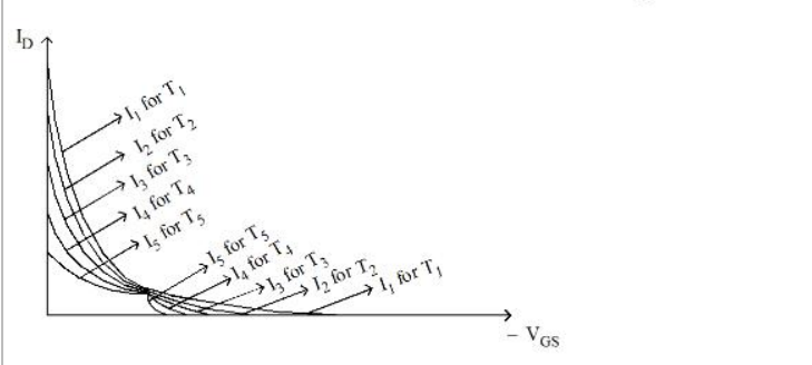
Choose the correct answer from the options given below :
When gate to source voltage of a FET changes from –5.2 volt to –5 volts, the corresponding drain current changes from 1 mA to 1.3 mA, the transconductance is
In a JFET the gate to source voltage is given as
In a JFET self-bias configuration shown below :
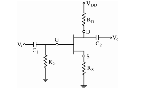
The drain current is
(a) \(K\dfrac{W}{L}(V_{gs}-V_{th})V_{ds}\)
(b) \(I_{DSS}\left(1-\dfrac{I_DR_S}{V_P}\right)^{2}\)
(c) \(I_{DSS}\left(1+\dfrac{I_DR_S}{V_P}\right)^{2}\)
(d) \(K\dfrac{W}{L}(V_{gs}-V_{th})^{2}\)
Out of these which are correct ?
Assertion (A) : FET is a device, which depends for its operation on the control of field or voltage due to applied current.
Reason (R) : FET has a very high input resistance of the order of mega-ohms. It is also immune to radiations.
Match the following :
List - I List - II (circuit in the original question) (a) JFET VGS = 0V (i) 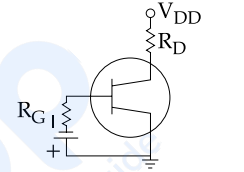
(b) JFET self-bias (ii) 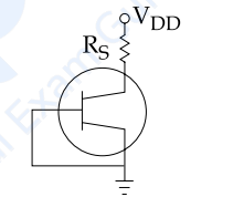
(c) JFET Fixed bias (iii) 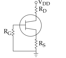
(d) FET Low Frequencies circuit (iv) 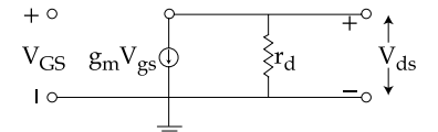
Codes :
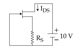
The JFET in a circuit shown in Figure, has an IDSS = 10 mA and Vp = − 5V. The value of resistance RS for a drain current IDS = 6.4 mA is (Choose the nearest value)
In a certain FET circuit, VGS = 0V, VDD = 15V, IDSS = 15 mA, and RD = 470Ω. If RD is decreased to 330 Ω, IDSS is :
Important Questions from Field Effect Transistors
Which of the following is the characteristic of Field-effect transistor?
- In junction field effect transistor, the drain current can be approximated as:
The expression for the transconductance (g m) of a JFET is:
Field Effect transistor is:
The main drawback of a JFET is its



