
For MOSFET, consider the following statements A. In triode region, FET works as voltage variable resistor B. For p-channel MOSFET, if VSG \(\gt\) |VTp|, then transistor will be in off mode C. Amplification factor is inversly proportional to the value of VGS/Vp. D. In saturation region, FET is used as amplifier. E. For depletion MOSFET, channel is diffused and current flows even if VGS is zero Choose the correct answer from the options given below :
A, D and E only
Each statement must be judged separately against MOSFET theory, and only the option containing exactly the true ones can be correct.
A — "In the triode region the FET works as a voltage variable resistor." TRUE. For small VDS the drain current is
\(I_D = k\left[(V_{GS}-V_T)V_{DS}-\dfrac{V_{DS}^{2}}{2}\right] \approx k(V_{GS}-V_T)V_{DS}\)
so the channel behaves as a resistance
\(r_{DS}=\dfrac{V_{DS}}{I_D}\approx\dfrac{1}{k(V_{GS}-V_T)}\)
whose value is set by the gate voltage — a voltage-controlled resistor, used in AGC circuits, analog switches and voltage-controlled attenuators.
B — "For a p-channel MOSFET, if VSG > |VTp| the transistor is OFF." FALSE. That inequality is precisely the turn-ON condition for a p-channel enhancement device: the gate must be sufficiently negative with respect to the source (i.e. VSG positive and larger than the threshold magnitude) to invert the surface and form the p-channel. The device is OFF when \(V_{SG} \lt |V_{Tp}|\).
C — "Amplification factor is inversely proportional to VGS/Vp." FALSE. The amplification factor is \(\mu = g_m r_d\), and the transconductance varies as
\(g_m = g_{m0}\left(1-\dfrac{V_{GS}}{V_p}\right)\)
This is a linear decrease with VGS/Vp, not an inverse (1/x) proportionality — the two are quite different dependences, and the statement as written is wrong.
D — "In the saturation region the FET is used as an amplifier." TRUE. Beyond pinch-off, \(I_D = \dfrac{k}{2}(V_{GS}-V_T)^{2}\) is almost independent of VDS, so the device acts as a voltage-controlled current source with high output resistance — exactly what linear amplification needs.
E — "For a depletion MOSFET the channel is diffused and current flows even at VGS = 0." TRUE. A depletion-type MOSFET is manufactured with a physically implanted/diffused channel between source and drain, so it is normally-ON and carries IDSS at zero gate bias; a negative gate depletes the channel and a positive gate enhances it, giving operation in both modes.
Collecting the true statements: A, D and E.
Hence, the correct answer is A, D and E only.
Similar Questions
In an FET, following characteristics are given :
1. JFET is called as variable current resistor.
2. JFET is called Voltage variable resistor.
3. \(g_{d}=g_{d0}\left(1-\dfrac{V_{GS}}{V_{P}}\right)\), where gd0 is value of drain to source conductance for zero bias.
4. \(g_{d}=g_{d0}\left(1+\dfrac{V_{GS}}{V_{P}}\right)^{2}\)Which one of the following is true ?
Transfer characteristics for n-channel FET as a function of temperature T is shown in the figure
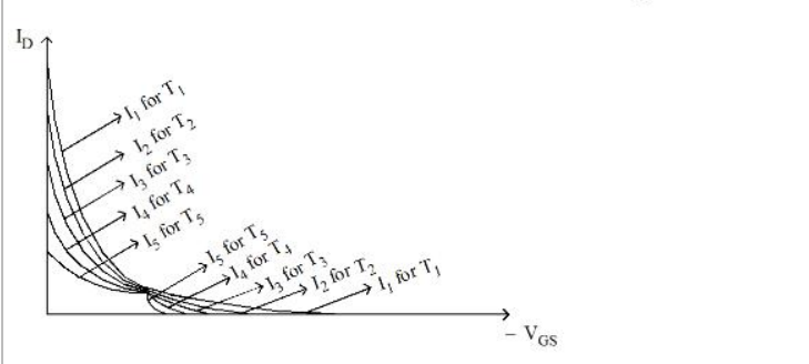
Choose the correct answer from the options given below :
When gate to source voltage of a FET changes from –5.2 volt to –5 volts, the corresponding drain current changes from 1 mA to 1.3 mA, the transconductance is
In a JFET the gate to source voltage is given as
In a JFET self-bias configuration shown below :
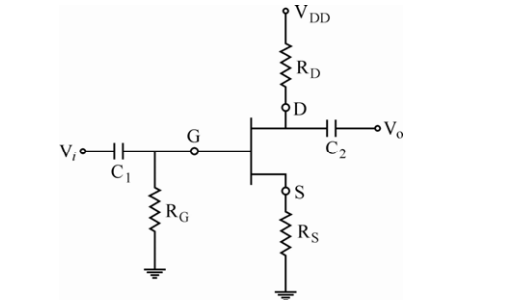
The drain current is
(a) \(K\dfrac{W}{L}(V_{gs}-V_{th})V_{ds}\)
(b) \(I_{DSS}\left(1-\dfrac{I_DR_S}{V_P}\right)^{2}\)
(c) \(I_{DSS}\left(1+\dfrac{I_DR_S}{V_P}\right)^{2}\)
(d) \(K\dfrac{W}{L}(V_{gs}-V_{th})^{2}\)
Out of these which are correct ?
Assertion (A) : FET is a device, which depends for its operation on the control of field or voltage due to applied current.
Reason (R) : FET has a very high input resistance of the order of mega-ohms. It is also immune to radiations.
Match the following :
List - I List - II (circuit in the original question) (a) JFET VGS = 0V (i) 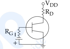
(b) JFET self-bias (ii) 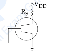
(c) JFET Fixed bias (iii) 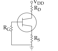
(d) FET Low Frequencies circuit (iv) 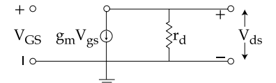
Codes :
Which of the following statements are valid for JFET ?
(a) \(I_{DS}=I_{DSS}\left(1-\dfrac{V_{GS}}{V_P}\right)\)
(b) \(I_{DS}=I_{DSS}\left(1+\dfrac{V_{GS}}{V_P}\right)\)
(c) \(\mu=\dfrac{g_m}{r_d}\)
(d) \(\mu=g_m\cdot r_d\)
Options :
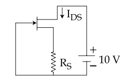
The JFET in a circuit shown in Figure, has an IDSS = 10 mA and Vp = − 5V. The value of resistance RS for a drain current IDS = 6.4 mA is (Choose the nearest value)
In a certain FET circuit, VGS = 0V, VDD = 15V, IDSS = 15 mA, and RD = 470Ω. If RD is decreased to 330 Ω, IDSS is :
Important Questions from Field Effect Transistors
Which of the following is the characteristic of Field-effect transistor?
- In junction field effect transistor, the drain current can be approximated as:
The expression for the transconductance (g m) of a JFET is:
Field Effect transistor is:
The main drawback of a JFET is its



