
Which of the following shows the proper biasing of a PNP transistor?
base and emitter - forward bias; collector and emitter - reverse bias
Understanding PNP Transistor Biasing
A bipolar junction transistor (BJT), like the PNP type, needs specific DC voltages applied to its terminals (Emitter, Base, and Collector) to operate correctly. This process is called biasing. The biasing sets up the operating point, also known as the Q-point, which determines how the transistor will behave when an AC signal is applied.
PNP Transistor Terminals and Operation
A PNP transistor is made of three layers of semiconductor material: a P-type emitter, an N-type base, and a P-type collector. The current flow direction is opposite to that in an NPN transistor. For a PNP transistor to amplify signals (operate in the active region), its two internal junctions must be biased in a particular way:
- The Base-Emitter junction must be forward biased.
- The Collector-Base junction must be reverse biased.
Let's consider the potential levels for these biasing conditions in a PNP transistor:
- For Base-Emitter forward bias: The P-type Emitter must be at a higher potential than the N-type Base. So, \(V_E > V_B\).
- For Collector-Base reverse bias: The P-type Collector must be at a lower potential than the N-type Base. So, \(V_C < V_B\).
Combining these conditions for active mode, we get \(V_C < V_B < V_E\).
Analyzing Biasing Options for PNP Transistors
The question presents biasing conditions in terms of "base and emitter" and "collector and emitter". While typically biasing is discussed as base-emitter and collector-base, let's interpret the given options:
- "base and emitter - forward bias": For a PNP, this means the Emitter is at a higher potential than the Base (\(V_E > V_B\)). This corresponds to forward biasing the Base-Emitter junction.
- "collector and emitter - reverse bias": For a PNP, this means the Collector is at a lower potential than the Emitter (\(V_C < V_E\)).
Now let's evaluate the given options:
- base and emitter - forward bias; collector and emitter - reverse bias:
- Base-Emitter: Forward bias (\(V_E > V_B\)). Correct for active mode.
- Collector-Emitter: Reverse bias (\(V_C < V_E\)). If Base-Emitter is forward biased (\(V_E > V_B\)) and Collector-Base is reverse biased (\(V_C < V_B\)), then it naturally follows that \(V_C\) will be significantly less than \(V_E\) (\(V_C << V_E\)), meaning the Collector is at a lower potential than the Emitter. This condition (\(V_C < V_E\)) is consistent with the active mode requirement (\(V_C < V_B < V_E\)). This option describes the correct conditions for active mode operation.
- base and emitter - forward bias; collector and emitter - forward bias:
- Base-Emitter: Forward bias (\(V_E > V_B\)). Correct for active mode.
- Collector-Emitter: Forward bias (\(V_C > V_E\)). This implies \(V_C > V_E > V_B\). This configuration typically corresponds to saturation mode, where both Base-Emitter and Collector-Base junctions are forward biased relative to the base potential.
- base and emitter - reverse bias; collector and emitter - forward bias:
- Base-Emitter: Reverse bias (\(V_E < V_B\)). This means the Base-Emitter junction is reverse biased, which corresponds to cutoff mode.
- Collector-Emitter: Forward bias (\(V_C > V_E\)). This combination does not fit standard operating modes.
- base and emitter - reverse bias; collector and emitter - reverse bias:
- Base-Emitter: Reverse bias (\(V_E < V_B\)). This means the Base-Emitter junction is reverse biased, which corresponds to cutoff mode.
- Collector-Emitter: Reverse bias (\(V_C < V_E\)). This combination reinforces the cutoff condition.
Therefore, the option that correctly describes the biasing for a PNP transistor to operate in its primary amplification mode (active region) is the one stating that the base and emitter are forward biased, and the collector and emitter are reverse biased, which implies the collector is at a significantly lower potential than the emitter.
Summary of PNP Operating Modes Biasing
| Operating Mode | Base-Emitter Junction | Collector-Base Junction | Potential Relationship (\(V_C\), \(V_B\), \(V_E\)) |
|---|---|---|---|
| Active (Amplification) | Forward Bias (\(V_E > V_B\)) | Reverse Bias (\(V_C < V_B\)) | \(V_C < V_B < V_E\) |
| Cutoff (Off Switch) | Reverse Bias (\(V_E < V_B\)) | Reverse Bias (\(V_C < V_B\)) | \(V_C < V_E < V_B\) or \(V_E < V_C < V_B\) |
| Saturation (On Switch) | Forward Bias (\(V_E > V_B\)) | Forward Bias (\(V_C > V_B\)) | \(V_C > V_B\) and \(V_E > V_B\) (often \(V_E \approx V_B\) and \(V_C \approx V_B\)) implies \(V_C \approx V_E \approx V_B\) (or \(V_E > V_B\), \(V_C > V_B\)) |
| Inverse Active | Reverse Bias (\(V_E < V_B\)) | Forward Bias (\(V_C > V_B\)) | \(V_E < V_B < V_C\) |
Based on this analysis, the first option correctly describes the biasing for active mode operation of a PNP transistor, interpreting "collector and emitter - reverse bias" as \(V_C < V_E\) when Base-Emitter is forward biased.
Revision Table: Transistor Biasing Modes
| Operating Mode | NPN Biasing (BE, CB) | PNP Biasing (BE, CB) |
|---|---|---|
| Active (Amplification) | Forward Bias, Reverse Bias | Forward Bias, Reverse Bias |
| Cutoff (Off Switch) | Reverse Bias, Reverse Bias | Reverse Bias, Reverse Bias |
| Saturation (On Switch) | Forward Bias, Forward Bias | Forward Bias, Forward Bias |
| Inverse Active | Reverse Bias, Forward Bias | Reverse Bias, Forward Bias |
Additional Information: Importance of Transistor Biasing
Proper biasing is crucial for any transistor circuit to function as intended. In amplification circuits, biasing ensures that the transistor operates within the linear portion of its characteristic curves (the active region). This allows the AC input signal to be amplified without significant distortion. Incorrect biasing can lead to the transistor operating in cutoff (no output signal) or saturation (clipped output signal), or even damage the device due to excessive current or voltage.
Different biasing techniques exist, such as fixed bias, collector-to-base bias, and voltage divider bias, each offering different levels of stability against variations in temperature or transistor parameters.
Similar Questions
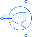
Identify the component shown in the image below:
The emitter current of a transistor is 1 mA. If 1% of the emitted current carriers are lost in the base recombination, what is the value β? Identify from the given options.
When the junction temperature of a transistor increases, its ______ increases.
The output impedance of a MOSFET is:
In a bipolar transistor, alpha is the ratio of:
Heat sink of a power transistor can be used for:
In case of an AC input signal in CE Transistor Load line can be given by a plot of
Which set of terminals is commonly used to connect a Field Effect Transistor in a circuit?
In an n-channel enhancement mode MOSFET, what must be applied to the gate terminal relative to the source to turn the device on?
What is the configuration called when the emitter terminal of a transistor is common to both input and output circuits?
Important Questions from Transistors
Transistors used as power amplifiers are generally mounted on a metallic plate so as to-
A transistor has ______ PN junctions
Which of the following is not true for a BJT?
A transistor amplifier with proper biasing has the following measured parameters:
Input resistance = 1 kΩ, Output resistance = 10 kΩ, Current gain = 90.
Identity the biasing configuration.
MOSFET can be used as a



