
Which set of terminals is commonly used to connect a Field Effect Transistor in a circuit?
Gate, Drain, Source
The question pertains to identifying the correct set of terminals used for connecting a Field Effect Transistor (FET) in a circuit. Let's evaluate each option:
- Emitter, Collector, Base: These terminals are associated with Bipolar Junction Transistors (BJTs), not FETs. BJTs rely on both electron and hole charge carriers.
- Positive, Negative, Neutral: These terms typically refer to electrical power supply polarities or three-phase AC power lines. They are not specifically related to transistors.
- Anode, Cathode, Grid: These terminals pertain to vacuum tubes and certain kinds of semiconductor devices like thyristors. They are not relevant to FETs.
- Gate, Drain, Source: These are the correct terminals for a Field Effect Transistor (FET). The "Gate" controls the channel conductivity between the "Source" and "Drain".
Based on the above explanations, the correct answer is Gate, Drain, Source as these are the standard terminal names used for FETs.
Explanation: In an FET, the Gate (G), Drain (D), and Source (S) are fundamental terminals:
- Gate: This terminal is used to control the current flowing between the Drain and Source. It does so by altering the electric field within the semiconductor.
- Drain: The terminal where current exits the transistor.
- Source: The terminal where current enters the transistor.
FETs are voltage-controlled devices, meaning that they are controlled by voltage applied to the Gate, as opposed to BJTs which are current-controlled.
Thus, Gate, Drain, Source is the correct set of terminals used for connecting a Field Effect Transistor in a circuit.
Similar Questions
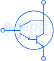
Identify the component shown in the image below:
The emitter current of a transistor is 1 mA. If 1% of the emitted current carriers are lost in the base recombination, what is the value β? Identify from the given options.
Heat sink of a power transistor can be used for:
In case of an AC input signal in CE Transistor Load line can be given by a plot of
How does the construction of a MOSFET help to achieve high input impedance?
While diagnosing an NPN BJT in a SOT-23 package, your multimeter positive probe (+) is locked on the Base (Pin 1). Measuring to Pin 3 reads 0.6 V, while measuring to Pin 2 reads 0.68 V. Which pin is the Emitter?
Which type of charge carriers mainly control current in a Field Effect Transistor (FET)?
What is the purpose of the base region in an NPN transistor?
Why are transistors preferred over mechanical switches for rapid switching operations?
In the output characteristics of a common-emitter configuration, a family of curves is obtained by varying VCE while keeping which quantity fixed? (Symbols have their usual meaning.)
Important Questions from Transistors
A transistor has ______ PN junctions
Which of the following is not true for a BJT?
A transistor amplifier with proper biasing has the following measured parameters:
Input resistance = 1 kΩ, Output resistance = 10 kΩ, Current gain = 90.
Identity the biasing configuration.
The change of output wave shape from the input wave shape of an amplifier is known as
Identify the component shown in the image below:



