
The output impedance of a MOSFET is:
The question asks about the typical output impedance of a MOSFET. The output impedance of a transistor is a crucial parameter that affects its performance in circuits, especially in amplifier configurations. It essentially describes how the output voltage changes in response to a change in output current.
Understanding MOSFET Output Impedance
Output impedance, denoted as \(Z_{out}\) or \(r_o\) (for small signal resistance), is the impedance seen looking back into the output terminals of a circuit. For a transistor like a MOSFET, this value depends significantly on the operating region of the device.
MOSFET Operating Regions and Output Impedance
A MOSFET operates in different regions depending on the applied gate-source voltage (\(V_{GS}\)) and drain-source voltage (\(V_{DS}\)). These regions are:
- Cutoff Region: The MOSFET is off, and essentially acts like an open circuit. The output impedance is very high, theoretically infinite.
- Triode (Linear) Region: The MOSFET acts like a voltage-controlled resistor. The output impedance is relatively low and varies with \(V_{GS}\).
- Saturation Region: The MOSFET acts like a current source whose current is primarily controlled by \(V_{GS}\) (and weakly by \(V_{DS}\) due to channel length modulation). This is the primary region for amplifier operation.
Why MOSFET Output Impedance is Extreme High in Saturation
In the saturation region, ideally, the drain current \(I_D\) is independent of \(V_{DS}\). This ideal behaviour corresponds to an infinite output impedance (\(r_o = \frac{\Delta V_{DS}}{\Delta I_D}\)). However, due to a phenomenon called channel length modulation, the channel effectively becomes slightly shorter as \(V_{DS}\) increases, causing a slight increase in \(I_D\). This non-ideal effect gives the MOSFET a finite, but still very high, output resistance in saturation.
The small-signal output resistance in the saturation region is typically denoted as \(r_o\) and can be approximated by the formula:
\(r_o = \frac{V_A}{I_D}\)
where \(V_A\) is the Early voltage (a parameter related to channel length modulation and device geometry) and \(I_D\) is the drain current. \(V_A\) is typically large compared to the operating voltages, and \(I_D\) is the DC bias current. This formula shows that \(r_o\) is inversely proportional to the drain current and directly proportional to the Early voltage.
Compared to the triode region where the output impedance is low (like a resistor), the saturation region exhibits a very high impedance, often in the range of tens or hundreds of kiloohms, or even megaohms for devices with long channels or high Early voltages.
Conclusion on MOSFET Output Impedance
While a MOSFET's output impedance varies with its operating region, when used in its typical application as an amplifier, it is biased in the saturation region. In this region, the small-signal output impedance is characteristic of a current source and is considered to be very high, often referred to as "extreme high impedance" when compared to other components or operating modes.
Revision Table: MOSFET Characteristics
| Characteristic | Typical Value (Saturation Region) | Notes |
|---|---|---|
| Input Impedance | Very High (ideally infinite) | Gate is insulated from channel |
| Output Impedance (\(r_o\)) | Extreme High | Due to channel length modulation |
| Transconductance (\(g_m\)) | Medium | Relates output current change to input voltage change |
Additional Information: MOSFET Amplifiers
The high output impedance of the MOSFET in saturation is beneficial in many amplifier designs, such as the common-source amplifier, as it contributes to a higher voltage gain. However, it can also be a limiting factor when driving low-impedance loads, often requiring additional buffer stages.
Similar Questions
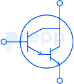
Identify the component shown in the image below:
The emitter current of a transistor is 1 mA. If 1% of the emitted current carriers are lost in the base recombination, what is the value β? Identify from the given options.
When the junction temperature of a transistor increases, its ______ increases.
Which of the following shows the proper biasing of a PNP transistor?
In a bipolar transistor, alpha is the ratio of:
Heat sink of a power transistor can be used for:
In case of an AC input signal in CE Transistor Load line can be given by a plot of
Which set of terminals is commonly used to connect a Field Effect Transistor in a circuit?
In an n-channel enhancement mode MOSFET, what must be applied to the gate terminal relative to the source to turn the device on?
What is the configuration called when the emitter terminal of a transistor is common to both input and output circuits?
Important Questions from Transistors
Transistors used as power amplifiers are generally mounted on a metallic plate so as to-
A transistor has ______ PN junctions
Which of the following is not true for a BJT?
A transistor amplifier with proper biasing has the following measured parameters:
Input resistance = 1 kΩ, Output resistance = 10 kΩ, Current gain = 90.
Identity the biasing configuration.
MOSFET can be used as a



