
The correct flow in the basic block diagram of op-Amp is A. Complementary symmetry push pull amplifier block. B. Dual input unbalanced output differential amplifier block C. Emitter follower with constant current source block D. Dual-Input balanced output differential amplifier block Choose the correct answer from the options given below :
D$\longrightarrow$ B$\longrightarrow$ C$\longrightarrow$A
To understand the correct flow in the basic block diagram of an Operational Amplifier (Op-Amp), it's important to know the function and interaction of each block mentioned in the options.
- Dual-Input Balanced Output Differential Amplifier Block (D): This is the first stage of the Op-Amp. It amplifies the difference between two input signals and is crucial for achieving a balanced output, which reduces noise and interference.
- Dual Input Unbalanced Output Differential Amplifier Block (B): This block typically follows the balanced differential amplifier. It serves the purpose of amplifying the input signal further but with one of the outputs grounded, thus providing an unbalanced output.
- Emitter Follower with Constant Current Source Block (C): Next in line, this block acts as a buffer offering high input impedance and low output impedance. It ensures that the previous stage does not get loaded, preserving signal integrity.
- Complementary Symmetry Push-Pull Amplifier Block (A): This is the final stage of the Op-Amp, which provides the necessary output power to drive the load efficiently. It uses both NPN and PNP transistors to provide high efficiency and low distortion.
Given the typical operation and arrangement of these blocks within the operational amplifier, the correct order as per the function is:
D (Dual-Input Balanced Output Differential Amplifier Block) → B (Dual Input Unbalanced Output Differential Amplifier Block) → C (Emitter Follower with Constant Current Source Block) → A (Complementary Symmetry Push-Pull Amplifier Block)
This order is logical as it starts with a stage that provides noise cancellation and continues with amplification and buffering necessary for driving the final output stage.
Thus, the correct answer is: D → B → C → A
Similar Questions
Assertion (A) : An Op-Amp is a direct coupled high gain amplifier.
Reason (R) : It consists of one or more differential amplifiers and usually followed by a level translator and push pull stage.
The input to a differentiator is –5 V. Its output will be
Match the following :
List – I List – II a. h-parameters i. O/P voltage varies as the slope of i/p voltage b. differentiator ii. Noise division c. half-wave rectifier iii. Function of a Q point d. integrator iv. series diode clipper Codes :
Assertion (A) : Op-Amp is used for sensor circuit.
Reason (R) : A small signal amplifier amplify weak measured signals.
For an inverting comparator circuit acting as a Schmitt Trigger, as shown in figure below, the expression of Hysteresis Voltage (Vny) is given by :
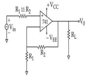
Consider the following statements :
(A) The output voltage of a summing amplifier (inverting configuration) with three inputs VA, VB and VC and input resistors RA, RB and RC is \(V_{o}=\left(1+\dfrac{R_{F}}{R_{A}R_{B}R_{C}}\right)\left[\dfrac{V_{A}}{R_{A}}+\dfrac{V_{B}}{R_{B}}+\dfrac{V_{C}}{R_{C}}\right]\)
(B) In a subtractor circuit, the output voltage is equal to voltage applied to non-inverting terminal minus voltage applied to inverting terminal
(C) The narrow band pass filter is called a Notch filter
(D) VCO is also called as frequency to voltage
(E) The all pass filter provides unity-gain with predictable phase shifts for different input frequenciesChoose the most appropriate answer from the options given below :
Consider the following circuit, the switch S1 allows the output to switch between two ranges of amplitudes from 0-0.1 V and 0-1 V. Arrange these values of R1, R2 and R3 in increasing order.
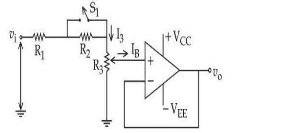
(A) Value of R1
(B) Value of R2
(C) Value of R3Choose the most appropriate answer from the options given below :
Match List I with List II
LIST I LIST II A. Butterworth filter of order '2' I. Impedance matching B. Buffer II. CMRR = ∞ (infinity) C. Schmitt Trigger III. Positive feedback D. Ideal OPAMP IV. 40 dB/decade roll off Choose the correct answer from the options given below:
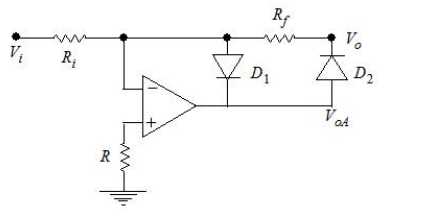
The given operational amplifier circuit corresponds to which electronic circuit application ?
Statements in connection to Op-Amp applications are :
A. If we use a square wave generator followed by integrator circuit we get a triangular wave at the output
B. The logarithmic amplifier called a log-amplifier or a logger, is basically a current to voltage converter.
C.
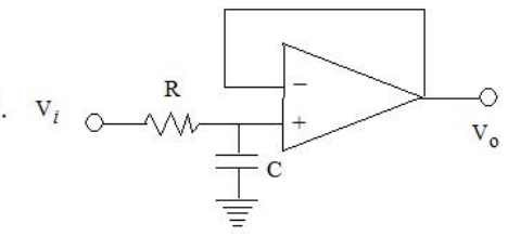 is a first order high pass filter with voltage follower
D. If we use a square wave generator followed by a clipping circuit then we get a saw-tooth wave generator.
Choose the correct answer from the options given below:
Important Questions from Op-Amp and Its Applications
An ideal Op-Amp is an ideal
- In an ideal OP-AMP, which one is correct?
Which of the following statements about the Op-Amp differential amplifiers is INCORRECT?
The input resistance of an ideal Op-Amp is
The input impedance of an ideal Op-amp is ______.



