Match the following : Codes :List - I List - II a) 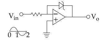
i) 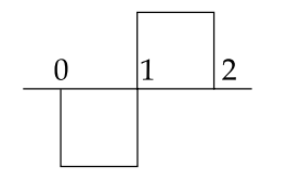
b) 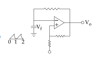
ii) 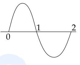
c) 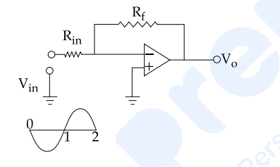
iii) 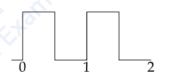
d) 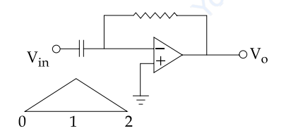
iv) 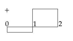
(a)-(iv), (b)-(iii), (c)-(ii), (d)-(i)
Identify each circuit by the element that sits in the feedback path — that element alone fixes the operation.
(c) is the anchor, so start there. A resistor in, a resistor back: the plain inverting amplifier with
\(V_{o}=-\dfrac{R_{f}}{R_{in}}V_{in}\)
A sine in gives a sine out, same shape, phase reversed. That is waveform (ii) — the inverted sine. This single link is decisive: only option 1 pairs (c) with (ii).
(d) capacitor in, resistor back — a differentiator.
\(V_{o}=-R_{f}C\dfrac{dV_{in}}{dt}\)
A triangular wave has a constant positive slope on the rise and a constant negative slope on the fall, so its derivative is a two-level square wave. With the triangle rising over 0 to 1 and falling over 1 to 2, the output flips sign at t = 1 — exactly waveform (i).
(a) a diode across the feedback path. The diode conducts on one polarity and blocks on the other, so the amplifier passes only half the input excursion and clips or level-shifts the rest. Fed with a sine, the output is a one-sided, clipped, essentially rectangular excursion sitting on a shifted level — waveform (iv).
(b) positive feedback through a divider with Vf on the other input — a Schmitt trigger. Positive feedback means the output can only sit at one saturation rail or the other, switching when the input crosses the upper or lower trip point
\(V_{UT},\ V_{LT}=\pm\dfrac{R_{2}}{R_{1}+R_{2}}V_{sat}\)
Fed with the rectified pulse train, it snaps between rails as each pulse crosses the threshold, producing the clean train of rectangular pulses — waveform (iii).
| Circuit | Feedback element | Function | Output |
|---|---|---|---|
| (a) | Diode | Clipper / precision rectifier | (iv) |
| (b) | Positive feedback divider | Schmitt trigger | (iii) |
| (c) | Resistor | Inverting amplifier | (ii) |
| (d) | Resistor with input C | Differentiator | (i) |
The general rule worth carrying away: resistor feedback scales, capacitor feedback integrates, a capacitor at the input differentiates, a diode rectifies or clips, and positive feedback turns the amplifier into a two-state switch.
Hence, the correct match is (a)-(iv), (b)-(iii), (c)-(ii), (d)-(i).
Similar Questions
Assertion (A) : An Op-Amp is a direct coupled high gain amplifier.
Reason (R) : It consists of one or more differential amplifiers and usually followed by a level translator and push pull stage.
The input to a differentiator is –5 V. Its output will be
Match the following :
List – I List – II a. h-parameters i. O/P voltage varies as the slope of i/p voltage b. differentiator ii. Noise division c. half-wave rectifier iii. Function of a Q point d. integrator iv. series diode clipper Codes :
Assertion (A) : Op-Amp is used for sensor circuit.
Reason (R) : A small signal amplifier amplify weak measured signals.
Consider the following circuit, the switch S1 allows the output to switch between two ranges of amplitudes from 0-0.1 V and 0-1 V. Arrange these values of R1, R2 and R3 in increasing order.
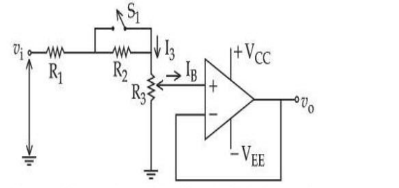
(A) Value of R1
(B) Value of R2
(C) Value of R3Choose the most appropriate answer from the options given below :
The given operational amplifier circuit corresponds to which electronic circuit application ?
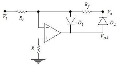
Statements in connection to Op-Amp applications are :
A. If we use a square wave generator followed by integrator circuit we get a triangular wave at the output
B. The logarithmic amplifier called a log-amplifier or a logger, is basically a current to voltage converter.
C.
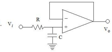 is a first order high pass filter with voltage follower
D. If we use a square wave generator followed by a clipping circuit then we get a saw-tooth wave generator.
Choose the correct answer from the options given below:
Match List I with List II
LIST I LIST II A. Single polarity positive voltage clipper circuit I. 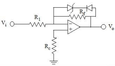
B. Negative clamping circuit II. 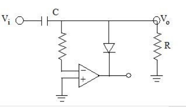
C. Differentiator circuit III. 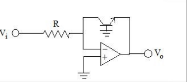
D. Logarithmic Amplifier IV. 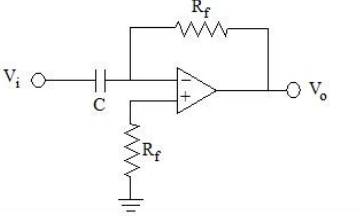
Choose the correct answer from the options given below:
The correct flow in the basic block diagram of op-Amp is
A. Complementary symmetry push pull amplifier block.
B. Dual input unbalanced output differential amplifier block
C. Emitter follower with constant current source block
D. Dual-Input balanced output differential amplifier block
Choose the correct answer from the options given below :
\(\dfrac{d^{2}y}{dt^{2}}+y=0\) can be solved using an Operational Amplifier. Which one is preferred ?
Important Questions from Op-Amp and Its Applications
In the circuit shown below, $R$ is $1\text{ k}\Omega$ and $R_f$ is $10\text{ k}\Omega$. If $V_{\text{in}}$ is $100\text{ mV}$ and the op-amps have supply voltages of $\pm 15\text{ V}$, then $V_{\text{out}}$ is _______ V.

For IC 741 circuit shown below, the maximum input frequency above which the output will be distorted is ____________.
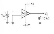
Assume that an op-amp 741 connected as a unit gain inverting amplifier is applied with an input change of 10 V. Determine the time taken for the output to change by 10 V. [Slew rate for op-amp 741 = 0.5 V/µs]
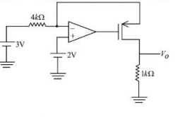
What is the value of output voltage $V_o$ in the given circuit? Assume op-amp to be ideal and MOSFET operating in saturation region.
In an ideal op-amp, the common mode gain is _____________.