
Assertion (A) : Op-Amp is used for sensor circuit. Reason (R) : A small signal amplifier amplify weak measured signals.
Both (A) and (R) are true and (R) is the correct explanation of (A).
Both are true, and the reason states exactly why the assertion holds — option 1.
How small sensor outputs actually are.
| Sensor | Output |
|---|---|
| Thermocouple | ~40 µV per °C |
| Strain gauge bridge | A few mV at full scale |
| ECG electrode | 1 – 2 mV |
| Photodiode | Nanoamps to microamps |
An ADC expects volts. Between the two sits an amplifier, and the op-amp is what fills the gap — usually as an instrumentation amplifier built from three of them.
Amplification is necessary but not sufficient, and the properties that make the op-amp the right choice all matter here:
Differential input with high CMRR. A bridge or a pair of electrodes delivers a small difference riding on a large common-mode voltage — mains hum, supply offset, the bridge's own excitation. A CMRR above 100 dB rejects what is common and keeps only the difference. A single-ended amplifier could not.
High input impedance. A sensor with a source impedance of megohms — a pH electrode, a piezoelectric transducer — would be loaded and its output attenuated by anything less. The op-amp draws picoamps.
Low offset and drift. Amplifying 40 µV by a thousand also amplifies the amplifier's own input offset voltage by a thousand. A chopper-stabilised device with 1 µV offset and nanovolt-per-degree drift is what makes microvolt measurement possible at all.
Direct coupling. Most sensor signals are DC or very slow, so the amplifier must respond down to zero frequency — which an op-amp does and a capacitively coupled amplifier does not.
The linkage is direct. The reason says weak signals need amplifying; the assertion says op-amps are used in sensor circuits; and it is precisely because sensor signals are weak that an op-amp is placed there. R explains A.
Beyond amplification, the same device also filters, linearises, converts current to voltage, and drives the ADC — but the reason names the primary function correctly.
Hence, both (A) and (R) are true and (R) is the correct explanation of (A).
Similar Questions
Assertion (A) : An Op-Amp is a direct coupled high gain amplifier.
Reason (R) : It consists of one or more differential amplifiers and usually followed by a level translator and push pull stage.
The input to a differentiator is –5 V. Its output will be
Match the following :
List – I List – II a. h-parameters i. O/P voltage varies as the slope of i/p voltage b. differentiator ii. Noise division c. half-wave rectifier iii. Function of a Q point d. integrator iv. series diode clipper Codes :
For an inverting comparator circuit acting as a Schmitt Trigger, as shown in figure below, the expression of Hysteresis Voltage (Vny) is given by :
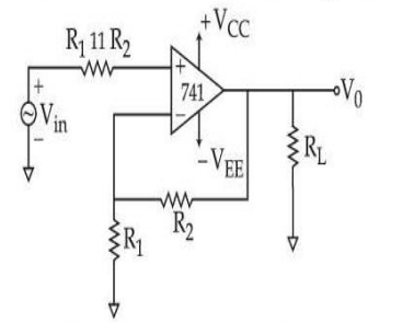
Consider the following statements :
(A) The output voltage of a summing amplifier (inverting configuration) with three inputs VA, VB and VC and input resistors RA, RB and RC is \(V_{o}=\left(1+\dfrac{R_{F}}{R_{A}R_{B}R_{C}}\right)\left[\dfrac{V_{A}}{R_{A}}+\dfrac{V_{B}}{R_{B}}+\dfrac{V_{C}}{R_{C}}\right]\)
(B) In a subtractor circuit, the output voltage is equal to voltage applied to non-inverting terminal minus voltage applied to inverting terminal
(C) The narrow band pass filter is called a Notch filter
(D) VCO is also called as frequency to voltage
(E) The all pass filter provides unity-gain with predictable phase shifts for different input frequenciesChoose the most appropriate answer from the options given below :
Consider the following circuit, the switch S1 allows the output to switch between two ranges of amplitudes from 0-0.1 V and 0-1 V. Arrange these values of R1, R2 and R3 in increasing order.
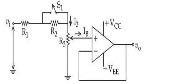
(A) Value of R1
(B) Value of R2
(C) Value of R3Choose the most appropriate answer from the options given below :
Match List I with List II
LIST I LIST II A. Butterworth filter of order '2' I. Impedance matching B. Buffer II. CMRR = ∞ (infinity) C. Schmitt Trigger III. Positive feedback D. Ideal OPAMP IV. 40 dB/decade roll off Choose the correct answer from the options given below:
The given operational amplifier circuit corresponds to which electronic circuit application ?
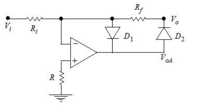
Statements in connection to Op-Amp applications are :
A. If we use a square wave generator followed by integrator circuit we get a triangular wave at the output
B. The logarithmic amplifier called a log-amplifier or a logger, is basically a current to voltage converter.
C.
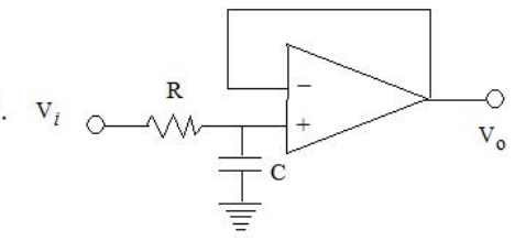 is a first order high pass filter with voltage follower
D. If we use a square wave generator followed by a clipping circuit then we get a saw-tooth wave generator.
Choose the correct answer from the options given below:
Match List I with List II
LIST I LIST II A. Single polarity positive voltage clipper circuit I. 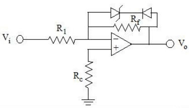
B. Negative clamping circuit II. 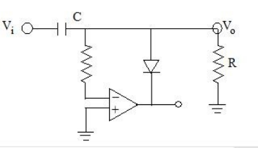
C. Differentiator circuit III. 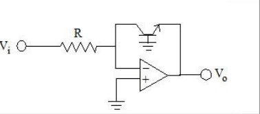
D. Logarithmic Amplifier IV. 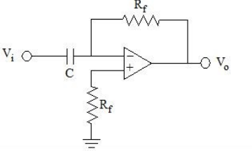
Choose the correct answer from the options given below:
Important Questions from Op-Amp and Its Applications
An ideal Op-Amp is an ideal
- In an ideal OP-AMP, which one is correct?
Which of the following statements about the Op-Amp differential amplifiers is INCORRECT?
The input resistance of an ideal Op-Amp is
The input impedance of an ideal Op-amp is ______.



