
The input to a differentiator is –5 V. Its output will be
0 V
A differentiator responds to change, and a steady –5 V does not change — so the output is 0 V, option 2.
\(V_{o}=-RC\dfrac{dV_{i}}{dt}\)
With \(V_{i}=-5\) V constant, \(\dfrac{dV_{i}}{dt}=0\), and the output is zero regardless of the values of R and C or of how large the input happens to be.
The circuit view says the same thing. The op-amp differentiator has a capacitor in series with the input and a resistor in the feedback path. The inverting terminal is a virtual earth, so the capacitor sees the full input voltage across it, and the current it passes is
\(i=C\dfrac{dV_{i}}{dt}\)
A capacitor blocks DC: once the initial transient has died away, a constant applied voltage drives no current. With no current through the feedback resistor there is no drop across it, and the output sits at the virtual-earth potential — zero.
| Input | Output |
|---|---|
| Constant (DC) | 0 V |
| Ramp, slope m | Constant, −RCm |
| Square wave | Sharp spikes at the edges |
| Sine, \(\sin\omega t\) | \(-RC\omega\cos\omega t\) — leads by 90° |
Why the sign of the input is irrelevant. Option 3 tempts by inverting the –5 V to +5 V, which is what an inverting amplifier of unit gain would do. But the differentiator's minus sign applies to the derivative, not to the input level; the DC value never reaches the output at all.
Options 1 and 4 invert the question. A square wave and a sine wave are what a differentiator produces from other inputs — spikes from a square wave, a cosine from a sine — not what it produces from a constant.
A practical footnote. The ideal differentiator's gain rises with frequency as \(\omega RC\), which amplifies high-frequency noise and threatens instability. Real circuits therefore add a small resistor in series with the input capacitor, so that above a chosen corner frequency the stage stops differentiating and behaves as a plain inverting amplifier. That modification does not alter the DC result: the series capacitor still blocks the steady input, and the output is still zero.
Hence, the output is 0 V.
Similar Questions
Assertion (A) : An Op-Amp is a direct coupled high gain amplifier.
Reason (R) : It consists of one or more differential amplifiers and usually followed by a level translator and push pull stage.
Match the following :
List – I List – II a. h-parameters i. O/P voltage varies as the slope of i/p voltage b. differentiator ii. Noise division c. half-wave rectifier iii. Function of a Q point d. integrator iv. series diode clipper Codes :
Assertion (A) : Op-Amp is used for sensor circuit.
Reason (R) : A small signal amplifier amplify weak measured signals.
For an inverting comparator circuit acting as a Schmitt Trigger, as shown in figure below, the expression of Hysteresis Voltage (Vny) is given by :
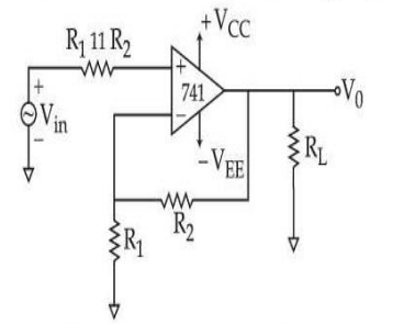
Consider the following statements :
(A) The output voltage of a summing amplifier (inverting configuration) with three inputs VA, VB and VC and input resistors RA, RB and RC is \(V_{o}=\left(1+\dfrac{R_{F}}{R_{A}R_{B}R_{C}}\right)\left[\dfrac{V_{A}}{R_{A}}+\dfrac{V_{B}}{R_{B}}+\dfrac{V_{C}}{R_{C}}\right]\)
(B) In a subtractor circuit, the output voltage is equal to voltage applied to non-inverting terminal minus voltage applied to inverting terminal
(C) The narrow band pass filter is called a Notch filter
(D) VCO is also called as frequency to voltage
(E) The all pass filter provides unity-gain with predictable phase shifts for different input frequenciesChoose the most appropriate answer from the options given below :
Consider the following circuit, the switch S1 allows the output to switch between two ranges of amplitudes from 0-0.1 V and 0-1 V. Arrange these values of R1, R2 and R3 in increasing order.
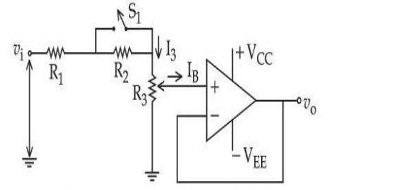
(A) Value of R1
(B) Value of R2
(C) Value of R3Choose the most appropriate answer from the options given below :
Match List I with List II
LIST I LIST II A. Butterworth filter of order '2' I. Impedance matching B. Buffer II. CMRR = ∞ (infinity) C. Schmitt Trigger III. Positive feedback D. Ideal OPAMP IV. 40 dB/decade roll off Choose the correct answer from the options given below:
The given operational amplifier circuit corresponds to which electronic circuit application ?
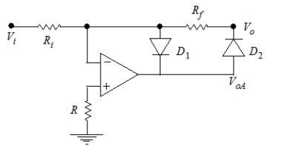
Statements in connection to Op-Amp applications are :
A. If we use a square wave generator followed by integrator circuit we get a triangular wave at the output
B. The logarithmic amplifier called a log-amplifier or a logger, is basically a current to voltage converter.
C.
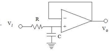 is a first order high pass filter with voltage follower
D. If we use a square wave generator followed by a clipping circuit then we get a saw-tooth wave generator.
Choose the correct answer from the options given below:
Match List I with List II
LIST I LIST II A. Single polarity positive voltage clipper circuit I. 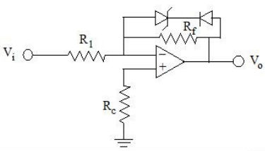
B. Negative clamping circuit II. 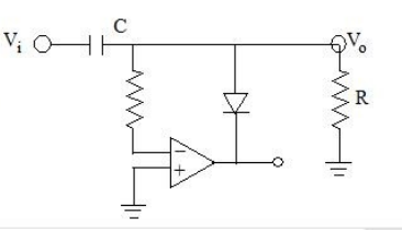
C. Differentiator circuit III. 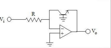
D. Logarithmic Amplifier IV. 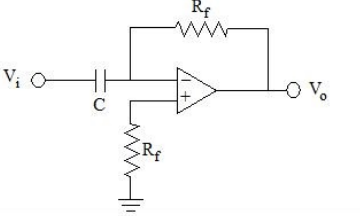
Choose the correct answer from the options given below:
Important Questions from Op-Amp and Its Applications
An ideal Op-Amp is an ideal
- In an ideal OP-AMP, which one is correct?
Which of the following statements about the Op-Amp differential amplifiers is INCORRECT?
The input resistance of an ideal Op-Amp is
The input impedance of an ideal Op-amp is ______.



