
Match the following lists : Choose the correct answer from the codes given below:List - I List - II a) 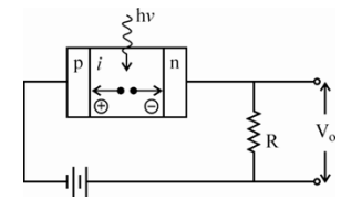
i) Solar cell b) 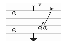
ii) Pn-photodiode c) 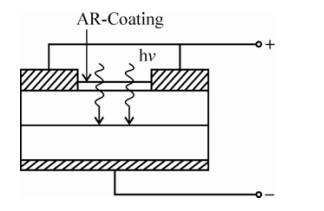
iii) Pin photodiode d) 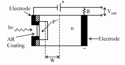
iv) Light emitting diode
a-iii, b-iv, c-i, d-ii
Two features identify every optoelectronic device drawn here: which way the light travels (in or out) and how the device is biased.
b → iv. Light emitting diode. The only structure with the light arrow pointing outward and with a forward bias applied. Forward bias injects carriers that recombine radiatively, emitting photons of energy \(h\nu\approx E_g\). Every other device in the list absorbs light; this one generates it.
c → i. Solar cell. Large area, anti-reflection coating, and crucially no external supply — just two terminals delivering power to the outside. That is photovoltaic operation: the light-generated carriers themselves develop the open-circuit voltage. The big area and AR coating are there to collect as much sunlight as possible, which is what distinguishes a solar cell from a photodiode.
a → iii. Pin photodiode. The layer stack is explicitly p–i–n, with the lightly doped intrinsic layer between the two doped regions, and it is reverse biased across a load resistor. The wide intrinsic region gives a thick depletion layer, so more photons are absorbed where the field can sweep the carriers out — high quantum efficiency and fast response.
d → ii. Pn-photodiode. A simple p+n junction, again reverse biased, with the depletion width W marked. There is no intrinsic layer, so W is fixed by the doping and the applied bias and cannot be tailored independently — the limitation that the p-i-n structure was invented to remove.
How to work through it quickly. Find the emitter first (light out, forward bias) → LED. Then find the one with no battery → solar cell. The two remaining reverse-biased detectors are separated by whether an intrinsic layer is drawn: with i-layer → p-i-n, without → p-n.
Hence, the correct matching is a-iii, b-iv, c-i, d-ii.
Similar Questions
Match the following :
List – I List – II a. LASER i. Emits monochromatic light of low intensity b. Solar cell ii. Consumes electrical power due to tHe incident light c. Photo diode iii. Delivers power to load d. LED iv. Emits monochromatic light of high intensity Codes :
Which one of the following is not LED material ?
1. Ga As
2. Ga P
3. Si
4. SiO2
When atoms in Direct bandgap semiconductors move from higher energy state (E2) to lower energy state (E1) and emission of light takes place, the energy of emitted photon is given as
Match the following :
List – I List – II a. LED i. Heavily doped b. Avalanche Photodiode ii. Coherent radiation c. Tunnel diode iii. Spontaneous emission d. LASER iv. Current gain Codes :
Match List I with List II
LIST I LIST II A. LED I. Photo resistive effect B. LCD II. Photo conductive effect C. LDR III. dynamic scattering of light D. Photo Diode IV. electro - luminescence Choose the correct answer from the options given below:
Which of the following statements are correct in case of Light Emitting Diodes ?
(a) Homojunctions LEDs are often surface emitters.
(b) Heterojunctions LEDs are Edge emitters.
(c) Heterojunction LEDs are often surface emitters.
(d) LEDs provide monochromatic & coherent radiations.
Options :
Arrange the below mentioned III-V materials to produce LEDs in order of their increasing emission wavelengths :
(a) In AS (b) Si C (c) Ga P (d) Ga AS
Codes :
The material LiNbO3 is used in the manufacturing of the following device :
Light emitting diodes fabricated from Ga, As emit radiations in the :
Important Questions from Optical Devices
An LCD requires a power of __________.
- The slope efficiency of a laser diode is 0.5 W/A, and the output optical power at a current of 100 mA is 30 mW. Assuming piece-wise linear characteristics of the laser diode, the threshold current of the laser is ________ mA.
- TV remote controls commonly use _____ to communicate with the TV.
- A DVD uses the _____ method to store and read data.
- The basic components of an optocoupler are _____.



