
Light emitting diodes fabricated from Ga, As emit radiations in the :
Infra - red region
The emitted wavelength is fixed by the band gap, so start there. When an electron in the conduction band recombines with a hole in the valence band, the photon carries away the band-gap energy:
\(E_{photon}=E_{g}=h\nu=\dfrac{hc}{\lambda}\)
which in practical units becomes the formula worth memorising:
\(\lambda\ (\mu\text{m})=\dfrac{1.24}{E_{g}\ (\text{eV})}\)
Apply it to gallium arsenide, whose band gap at room temperature is 1.42 eV:
\(\lambda=\dfrac{1.24}{1.42}=0.873\ \mu\text{m}=873\ \text{nm}\)
The visible spectrum ends at about 700 nm, so 873 nm lies clearly in the near infra-red — option 4.
| Material | Eg | λ | Colour |
|---|---|---|---|
| GaAs | 1.42 eV | 873 nm | Infra-red |
| GaAsP | 1.9 eV | 650 nm | Red |
| GaP | 2.26 eV | 550 nm | Green |
| GaN | 3.4 eV | 365 nm | Blue / UV |
Why GaAs is used for LEDs at all, despite being invisible: it is a direct band-gap material. An electron at the bottom of the conduction band sits directly above a hole at the top of the valence band in momentum space, so recombination needs no phonon to conserve momentum and the transition is fast and efficient. Silicon and germanium are indirect, which is why they make excellent detectors but hopeless emitters.
Where the infra-red output is exactly what is wanted. GaAs emitters drive remote controls, optocouplers, IR proximity and obstacle sensors, and the first generation of short-haul fibre links — silicon photodiodes happen to be most sensitive near 850 nm, so detector and emitter match beautifully.
To move into the visible, the band gap must be widened, which is done by alloying: adding phosphorus to give GaAsP shifts the emission through red and amber, and GaP reaches green. Longer wavelengths for long-haul fibre (1310 and 1550 nm) come from InGaAsP, whose gap is narrower still.
Hence, GaAs LEDs emit in the infra-red region.
Similar Questions
Match the following :
List – I List – II a. LASER i. Emits monochromatic light of low intensity b. Solar cell ii. Consumes electrical power due to tHe incident light c. Photo diode iii. Delivers power to load d. LED iv. Emits monochromatic light of high intensity Codes :
Which one of the following is not LED material ?
1. Ga As
2. Ga P
3. Si
4. SiO2
When atoms in Direct bandgap semiconductors move from higher energy state (E2) to lower energy state (E1) and emission of light takes place, the energy of emitted photon is given as
Match the following :
List – I List – II a. LED i. Heavily doped b. Avalanche Photodiode ii. Coherent radiation c. Tunnel diode iii. Spontaneous emission d. LASER iv. Current gain Codes :
Match List I with List II
LIST I LIST II A. LED I. Photo resistive effect B. LCD II. Photo conductive effect C. LDR III. dynamic scattering of light D. Photo Diode IV. electro - luminescence Choose the correct answer from the options given below:
Match the following lists :
List - I List - II a) 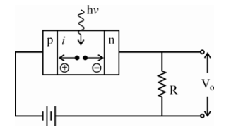
i) Solar cell b) 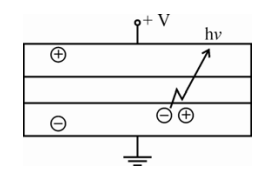
ii) Pn-photodiode c) 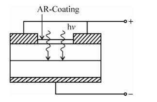
iii) Pin photodiode d) 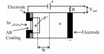
iv) Light emitting diode Choose the correct answer from the codes given below:
Which of the following statements are correct in case of Light Emitting Diodes ?
(a) Homojunctions LEDs are often surface emitters.
(b) Heterojunctions LEDs are Edge emitters.
(c) Heterojunction LEDs are often surface emitters.
(d) LEDs provide monochromatic & coherent radiations.
Options :
Arrange the below mentioned III-V materials to produce LEDs in order of their increasing emission wavelengths :
(a) In AS (b) Si C (c) Ga P (d) Ga AS
Codes :
The material LiNbO3 is used in the manufacturing of the following device :
Important Questions from Optical Devices
An LCD requires a power of __________.
- The slope efficiency of a laser diode is 0.5 W/A, and the output optical power at a current of 100 mA is 30 mW. Assuming piece-wise linear characteristics of the laser diode, the threshold current of the laser is ________ mA.
- TV remote controls commonly use _____ to communicate with the TV.
- A DVD uses the _____ method to store and read data.
- The basic components of an optocoupler are _____.



