
Flip Flop can be used to make : (a) Latches (b) Bounce-elimination switches (c) ADDER (d) Encoder Which of the statements given above are correct ?
(a) and (b) only
The dividing line is memory. A flip-flop is a one-bit storage element, so it can only build things that need to remember. Sort the four candidates on that test and the answer follows at once.
| Item | Needs memory? | Built from a flip-flop? |
|---|---|---|
| (a) Latch | Yes | Yes |
| (b) Bounce-elimination switch | Yes | Yes |
| (c) Adder | No | No — combinational |
| (d) Encoder | No | No — combinational |
So (a) and (b), which is option 1.
(a) Latches. The latch is the flip-flop's own ancestor: two cross-coupled NOR or NAND gates form an SR latch that holds one bit indefinitely. A flip-flop is the same structure with clocking added, so the two are intimately related — a D flip-flop is literally a pair of D latches in a master-slave arrangement.
(b) Bounce-elimination switches, and why memory is essential here. A mechanical contact does not close cleanly; it chatters for several milliseconds, which a fast logic gate reads as a burst of pulses. A single-pole double-throw switch feeding an SR latch cures it completely: the first contact sets the latch, and all subsequent bounces on that same terminal find the latch already in that state and change nothing. The output is one clean transition. No combinational circuit can do this, because it has no way of knowing that the first edge has already been seen.
Why (c) and (d) cannot be right. An adder's output depends only on its present inputs — the same A, B and carry-in always give the same sum, with no history involved. So it is built from XOR and AND gates alone. An encoder likewise maps an active input line to a binary code by pure combinational logic. Neither has any state to store.
The one caveat worth noting. A serial adder does contain a flip-flop — but only to hold the carry between successive bit times, which is a storage function bolted onto a combinational full adder. The adder proper remains combinational.
What flip-flops actually build. Registers, shift registers, counters, frequency dividers, sequence detectors and the state memory of every finite state machine — the sequential half of digital design.
Hence, the correct statements are (a) and (b).
Similar Questions
Read the following statements :
i. Gate is a combinational logic.
ii. JK Flip-flop in toggle mode is not combinational logic.
iii. MSJK FF suffers from race-around.
iv. Counters are sequential circuits.Which is correct ?
Which flip-flop can be used as latch ?
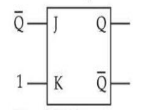
In a J-K FF, if J = Q and K = 1 (see figure). Assuming the flip flop was initially cleared and then clocked for 6 pulses, the sequence at the Q output will be :
Consider the following statements regarding registers and latches :
(A) Registers are made of edge triggered flip-flops whereas latches are made from level triggered flip flops
(B) Registers are temporary storage devices whereas latches are not
(C) A latch employs cross coupled feed back connections
(D) A register stores a binary word whereas a latch does notChoose the most appropriate answer from the options given below :
The toggle condition appears in J-K flip-flop when
A. J=1, K=1
B. J=0, K=0
C. J=0, K=1
D. J=1, K=0
E. J=0, K=1 and J=1, K=0
Choose the correct answer from the options given below :
Match List I with List II
LIST I (Diagram) LIST II (Sequential Circuit) A. 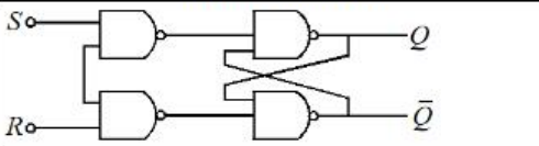
I. Edge triggered S-R flip flop B. 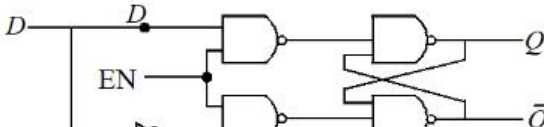
II. D Flip flop to SR flip flop C. 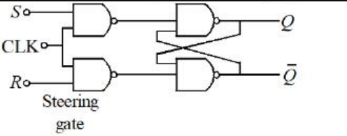
III. Gated Latch clocked flip flop D. 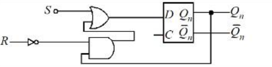
IV. Gated D Latch Choose the correct answer from the options given below:
The truth table of D flip-flop is given below:
C D Qn+1 O X Qn (Last State) $\uparrow$ 0 0 $\uparrow$ 1 1 Choose exact characteristic equation based on above Truth Table
Assertion (A) : Delay flip flop is used to store a single bit either 0 or 1.
Reason (R) : It has only one input, when clock is high and D input is also high, the output resets.
Assertion (A) : Asynchronous sequential circuit is also called event driven circuit.
Reason (R) : Event driven circuit does not have clock to trigger change of state. The states are changed by the change in input signal of the previous stage.
Select your answer using the codes given below.
For the circuit shown below consider the two statements :
Assertion (A) : The circuit is sequential.
Reason (R) : There is a loop in circuit.
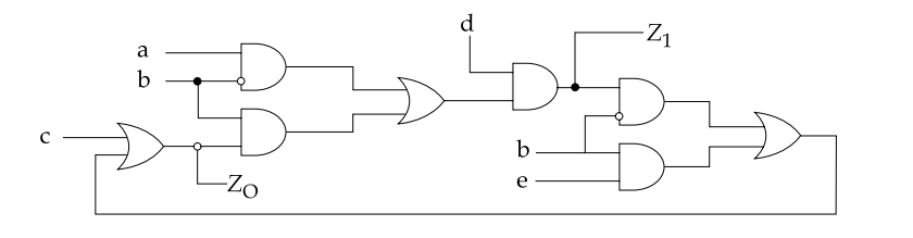
Select your answer using the codes given below.
Important Questions from Sequential Circuits
The basic sequential logic building block in which the output follows the data input as long as the ENABLE input is active, is
What can be the maximum clock frequency of a 10-bit ripple counter which will not cause a count to skip, considering 10 ns propagation delay for each of the edge-triggered flip flops?
The output of a sequential circuit depends on
The basic building block of a sequential logic circuit is
A 4bit synchronous counter uses flip-flops with a propagation delay time of 25ns each. The maximum possible time required for change of state will be



