
Read the following statements : (a) In a J-K Flip Flop, if J = K, the resulting Flip Flop is referred to as a T-type Flip Flop Which is correct ?
(b) In a J-K Flip Flop, if J ≠ K, the resulting Flip Flop is referred to as a D-type Flip Flop
(c) An S-R Flip Flop cannot be converted into a T-type Flip Flop since S = R = 1 is not allowed.
(a) and (b)
The J-K flip-flop is the universal one: tie its inputs together in the two possible ways and the other two types fall out.
(a) J tied to K gives a T flip-flop — correct. With a single input T driving both,
\(Q_{n+1}=T\overline{Q_{n}}+\overline{T}Q_{n}=T\oplus Q_{n}\)
so T = 0 holds the state and T = 1 toggles it — exactly the T flip-flop, the building block of every counter.
(b) J and K made complementary gives a D flip-flop — correct. Setting \(J=D\) and \(K=\overline{D}\) in the characteristic equation,
\(Q_{n+1}=D\overline{Q_{n}}+\overline{\overline{D}}Q_{n}=D\overline{Q_{n}}+DQ_{n}=D\)
The output simply follows the input at each clock edge — the D or "data" flip-flop, made from a J-K with a single inverter. The statement's "J ≠ K" is loose phrasing for this complementary connection, which is the only way two binary inputs can differ.
So (a) and (b) hold, giving option 1.
(c) is the questionable statement. It is true that S = R = 1 is forbidden in an S-R flip-flop, and true that this is why a bare S-R cannot toggle. But "cannot be converted" is too strong: the conversion is standard and uses the outputs as feedback,
\(S=T\overline{Q}\qquad R=TQ\)
Because Q and \(\overline{Q}\) are always complementary, S and R can never both be 1, and with T = 1 exactly one of them is active — precisely the one that flips the state. That is in fact how the J-K flip-flop itself is built. Since a conversion does exist, (c) is best read as false, and the answer is flagged for confirmation because a key that reads (c) as a statement about the bare S-R would mark it true.
| Conversion | Connection | Result |
|---|---|---|
| J-K → T | J = K = T | \(Q_{n+1}=T\oplus Q_{n}\) |
| J-K → D | J = D, K = D̄ | \(Q_{n+1}=D\) |
| S-R → T | S = TQ̄, R = TQ | Toggles, invalid state impossible |
The general method for any conversion is the same: write the excitation table of the available flip-flop, the required next-state behaviour of the target, and use a K-map to express the available inputs in terms of the target's input and the present state.
Hence, the correct statements are (a) and (b).
Similar Questions
Read the following statements :
i. Gate is a combinational logic.
ii. JK Flip-flop in toggle mode is not combinational logic.
iii. MSJK FF suffers from race-around.
iv. Counters are sequential circuits.Which is correct ?
Which flip-flop can be used as latch ?
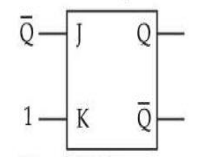
In a J-K FF, if J = Q and K = 1 (see figure). Assuming the flip flop was initially cleared and then clocked for 6 pulses, the sequence at the Q output will be :
Consider the following statements regarding registers and latches :
(A) Registers are made of edge triggered flip-flops whereas latches are made from level triggered flip flops
(B) Registers are temporary storage devices whereas latches are not
(C) A latch employs cross coupled feed back connections
(D) A register stores a binary word whereas a latch does notChoose the most appropriate answer from the options given below :
The toggle condition appears in J-K flip-flop when
A. J=1, K=1
B. J=0, K=0
C. J=0, K=1
D. J=1, K=0
E. J=0, K=1 and J=1, K=0
Choose the correct answer from the options given below :
Match List I with List II
LIST I (Diagram) LIST II (Sequential Circuit) A. 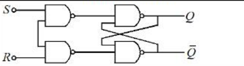
I. Edge triggered S-R flip flop B. 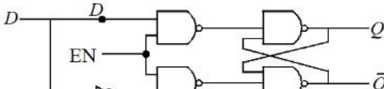
II. D Flip flop to SR flip flop C. 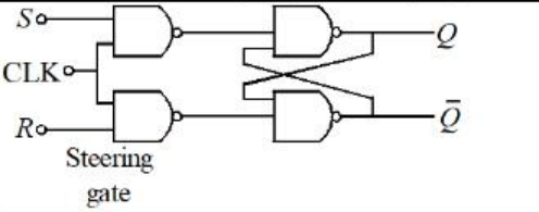
III. Gated Latch clocked flip flop D. 
IV. Gated D Latch Choose the correct answer from the options given below:
The truth table of D flip-flop is given below:
C D Qn+1 O X Qn (Last State) $\uparrow$ 0 0 $\uparrow$ 1 1 Choose exact characteristic equation based on above Truth Table
Assertion (A) : Delay flip flop is used to store a single bit either 0 or 1.
Reason (R) : It has only one input, when clock is high and D input is also high, the output resets.
Assertion (A) : Asynchronous sequential circuit is also called event driven circuit.
Reason (R) : Event driven circuit does not have clock to trigger change of state. The states are changed by the change in input signal of the previous stage.
Select your answer using the codes given below.
For the circuit shown below consider the two statements :
Assertion (A) : The circuit is sequential.
Reason (R) : There is a loop in circuit.
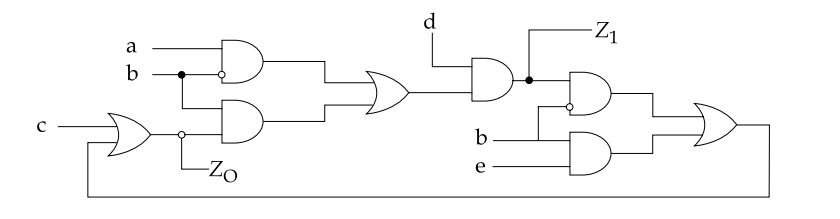
Select your answer using the codes given below.
Important Questions from Sequential Circuits
The basic sequential logic building block in which the output follows the data input as long as the ENABLE input is active, is
What can be the maximum clock frequency of a 10-bit ripple counter which will not cause a count to skip, considering 10 ns propagation delay for each of the edge-triggered flip flops?
The output of a sequential circuit depends on
The basic building block of a sequential logic circuit is
A 4bit synchronous counter uses flip-flops with a propagation delay time of 25ns each. The maximum possible time required for change of state will be



