
The basic purpose of biasing a transistor with a network is
to improve the stability
The words "with a network" are the key to the question. Any single resistor can place the operating point somewhere; what a bias network adds is the ability to hold that point steady — option 3.
What the operating point is fighting against. Two things move it, and both are outside the designer's control:
The spread of \(\beta\). Devices of the same part number vary by three to one, so a bias scheme that fixes \(I_{B}\) and relies on \(I_{C}=\beta I_{B}\) gives a different collector current in every unit built.
Temperature. The leakage current \(I_{CBO}\) roughly doubles for each 10 °C rise and is multiplied inside the transistor:
\(I_{CEO}=(1+\beta)I_{CBO}\)
and \(V_{BE}\) falls by about 2 mV/°C, which by itself raises the current further. Both effects heat the device, which increases the current again — the positive loop known as thermal runaway.
| Scheme | Stability factor S |
|---|---|
| Fixed bias | \(1+\beta\) — the worst possible |
| Collector-to-base bias | Intermediate |
| Voltage-divider with RE | \(\dfrac{1+\beta}{1+\beta\dfrac{R_{E}}{R_{E}+R_{TH}}}\approx1+\dfrac{R_{TH}}{R_{E}}\) |
How the network achieves it. A divider holds the base at a fixed voltage while an emitter resistor senses the actual emitter current and feeds a correction back:
\(I_{C}\uparrow\ \Rightarrow\ V_{E}\uparrow\ \Rightarrow\ V_{BE}\downarrow\ \Rightarrow\ I_{B}\downarrow\ \Rightarrow\ I_{C}\downarrow\)
The result is a stability factor of a few units instead of \(1+\beta\), and an operating point that depends on resistor ratios rather than on the transistor.
Why the other options fail. Reducing dissipation is not the aim — biasing deliberately establishes a quiescent current, and hence quiescent dissipation. Gain follows from the chosen operating point, but a bias network's job is to keep it there, not to raise it; indeed the emitter resistor reduces AC gain unless bypassed. Frequency response is governed by the coupling and bypass capacitors and the device's own capacitances, not by the bias network.
Hence, the basic purpose is to improve the stability.
Similar Questions
Assertion (A) : A self-biased circuit has a better stability than a fixed bias circuit.
Reason (R) : It provides negative feed back by the use of an additional resistor between the base and ground.
For an Emitter Bias BJT configuration arrange stability factor S(Iw) in descending order if β = 50. RB is base resistance and RE is emitter resistance.
(A) RE = 0.1 RB
(B) RB = 60 RE
(C) RB = 100 RE
(D) RE = 10 RB
(E) RB = 30 REChoose the most appropriate answer from the options given below :
The quienscent state of transistor is when
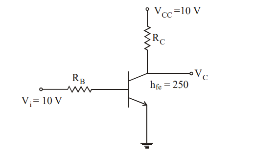
For a transistor inverter shown below, if IC sat is 10 mA, the value of RB and RC are
Assertion (A) : The bias instability occurs in transistors due to thermal variations.
Reason (R) : The reverse saturation current doubles for every 18 °C temperature rise. Due to this the reverse saturation current further heats the junction. As a result there is a thermal run-away.
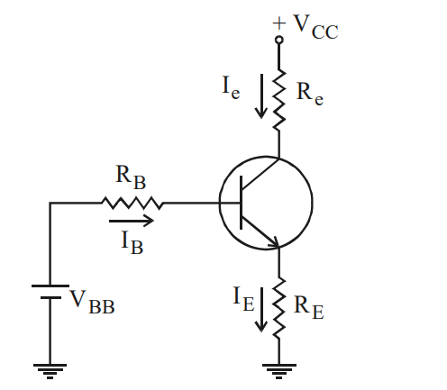
In a circuit given below the base current IB is
Assertion (A) : Completion of the design in a transistor requires the check of quiescent-point variations due to temperature changes and unit to unit parameter differences.
Reason (R) : As the principle of operation of the BJT & FET differ, so do the associated methods of Q-point stabilization.
Select your answer using the codes given below :
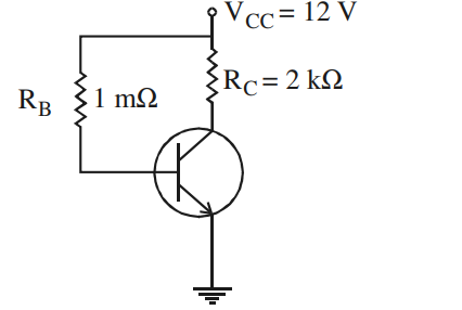
In a circuit shown below, the base current is
Important Questions from Biasing of Transistors
What is the operating point of a transistor as an amplifier known as?
When no ac input signals are connected to CE Transistor Load line can be plotted ______
In how many regions can the biased transistor work?
In a BJT, if the base-emitter junction is reverse-biased and the base-collector junction is reverse-biased, it is said to operate in
When transistors are used in digital circuits they usually operate in the:



