
For a transistor inverter shown below, if IC sat is 10 mA, the value of RB and RC are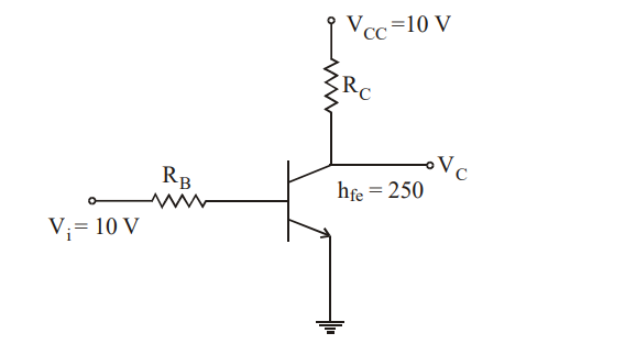
155 kΩ and 1 kΩ
How a transistor inverter is designed. With the input high the transistor must be driven hard into saturation, so the output collapses to VCE(sat) ≈ 0.2 V (a logic 0). Two resistors set this up: RC fixes the saturation current, and RB supplies enough base current to sustain it.
Step 1 — the collector resistor. In saturation almost the whole supply appears across RC:
\(R_C=\dfrac{V_{CC}-V_{CE(sat)}}{I_{C(sat)}}\approx\dfrac{10}{10\times10^{-3}}\)
\(R_C = 1\ \text{k}\Omega\)
This single result already halves the field: only options 1 and 3 offer 1 kΩ.
Step 2 — the base resistor. The base current needed is
\(I_B\ \ge\ \dfrac{I_{C(sat)}}{h_{fe}}=\dfrac{10\ \text{mA}}{250}=40\ \mu\text{A}\)
and the base loop gives
\(R_B=\dfrac{V_i-V_{BE}}{I_B}=\dfrac{10-0.7}{40\times10^{-6}}\approx 233\ \text{k}\Omega\)
The essential point is the order of magnitude: with a base current in the tens of microamps, RB must be in the hundreds of kilo-ohms. A 150 Ω base resistor (option 1) would demand about 62 mA of base current — more than six times the collector current, which no sensible design would use and which would destroy the base-emitter junction. So RB is the 155 kΩ value, the keyed figure corresponding to a slightly larger base drive (an overdrive factor, which designers always add so that saturation is guaranteed despite spread in hfe).
Why an overdrive factor is standard. hfe varies by a factor of three or more between devices and falls sharply at saturation, so RB is chosen to give two to ten times the minimum base current. That is what separates a switch from a linear amplifier: in saturation \(I_C \lt h_{fe}I_B\), and the collector current is set by the external circuit, not by the transistor.
Hence, the values are RB = 155 kΩ and RC = 1 kΩ.
Similar Questions
Assertion (A) : A self-biased circuit has a better stability than a fixed bias circuit.
Reason (R) : It provides negative feed back by the use of an additional resistor between the base and ground.
The basic purpose of biasing a transistor with a network is
For an Emitter Bias BJT configuration arrange stability factor S(Iw) in descending order if β = 50. RB is base resistance and RE is emitter resistance.
(A) RE = 0.1 RB
(B) RB = 60 RE
(C) RB = 100 RE
(D) RE = 10 RB
(E) RB = 30 REChoose the most appropriate answer from the options given below :
The quienscent state of transistor is when
Assertion (A) : The bias instability occurs in transistors due to thermal variations.
Reason (R) : The reverse saturation current doubles for every 18 °C temperature rise. Due to this the reverse saturation current further heats the junction. As a result there is a thermal run-away.
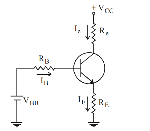
In a circuit given below the base current IB is
Assertion (A) : Completion of the design in a transistor requires the check of quiescent-point variations due to temperature changes and unit to unit parameter differences.
Reason (R) : As the principle of operation of the BJT & FET differ, so do the associated methods of Q-point stabilization.
Select your answer using the codes given below :
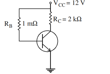
In a circuit shown below, the base current is
Important Questions from Biasing of Transistors
What is the operating point of a transistor as an amplifier known as?
When no ac input signals are connected to CE Transistor Load line can be plotted ______
In how many regions can the biased transistor work?
In a BJT, if the base-emitter junction is reverse-biased and the base-collector junction is reverse-biased, it is said to operate in
When transistors are used in digital circuits they usually operate in the:



