8085 Bus Technique for Memory and I/O Access
The Intel 8085 microprocessor employs a specific method to handle communication pathways for both memory and I/O devices, focusing on pin efficiency.
Multiplexed Address/Data Bus Explained
The core technique used by the 8085 is the multiplexed address/data bus. This approach uses a single set of pins for transmitting both the address and the data, but sequentially.
- Initially, the 8085 outputs the memory or I/O address on the pins AD0 through AD7 (along with A8-A15 for the full 16-bit address).
- The Address Latch Enable (ALE) signal indicates that the lower 8 bits on AD0-AD7 represent the address. An external latch captures this address.
- After the ALE signal goes low, the same pins (AD0-AD7) are repurposed for data transfer (reading from or writing to the selected location/device).
This multiplexing reduces the total number of pins needed for the processor.
Analysis of Alternatives
- Separate memory and I/O buses: The 8085 uses control signals (like IO/M̅) to differentiate between memory and I/O operations, but it shares the physical address/data lines, unlike systems with truly separate buses for each.
- Harvard architecture: The 8085 follows the Von Neumann architecture, having a unified address space for both instructions and data, distinct from the Harvard architecture's separate spaces.
- Fully asynchronous bus: The 8085 bus operations are timed using specific control signals (RD̅, WR̅, ALE, etc.), making it synchronous or partially asynchronous, not fully asynchronous where transfers complete purely based on device readiness without strict timing coordination.
Consequently, the defining technique for memory and I/O access in the 8085 is its multiplexed bus structure.
Similar Questions
- Calculate the output voltage of an op-amp for input voltages of $V_{i1} = 150 \mu\text{V}$ and $V_{i2} = 140 \mu\text{V}$. The amplifier has a differential gain of $A_d = 4000$ and the value of CMRR is $100$ :
- For an op-amp having a slew rate of $4\text{ V}/\mu\text{s}$, what is the maximum closed-loop voltage gain that can be used when input signal varies by $0.1\text{V}$ in $10\mu\text{s}$ ?
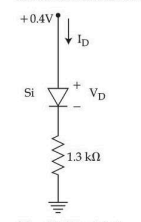
For the series diode configuration of the given figure, determine $V_D$ and $I_D$.
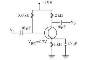
For the given emitter-bias network, determine the values of $I_C$ and $V_{CE}$. Assume $\beta = 100$.
- Given below are two statements : one is labelled as Assertion (A) and the other is labelled as Reason (R).
Assertion (A) : The gate of a MOSFET is insulated from body of FET by deposition of a very thin fragile layer of $\text{SiO}_2$ over the substrate.
Reason (R) : The device is therefore called an insulated gate field-effect transistor (IGFET).
In the light of the above statements, choose the most appropriate answer from the options given below : - If 8085 microprocessor adds 87H and 79H, then :
- The content of register (B) and register (C) of 8085 microprocessor are 0AH and 0BH. It is desired to multiply the content of register B and register C and store the results in accumulator. A part of 8085 program for this purpose is given as :
MVI A, 00H
LOOP ; _ _ _ _ _
_ _ _ _ _ _ _ _ _
_ _ _ _ _ _ _ _ _
HLT END
A sequence of instructions to complete the program would be : - The sequence of steps performed by microprocessor to fetch the data byte from memory :
A. The byte is placed in the instruction decoder of the microprocessor.
B. The byte from the memory location is placed on data bus.
C. The control unit sends the control signal $\overline{\text{RD}}$ to enable the memory chip.
D. The microprocessor places the 16-bit memory address from program counter on the address bus.
Choose the correct answer from the options given below : - Sequence of steps in 8085 microprocessor interrupt execution :
A. Interrupt acknowledged
B. Program counter content saved
C. Control transfered to ISR
D. Interrupt vector is read
Choose the correct answer from the options given below : - Consider the following statements regarding the 8085 microprocessor :
A. The 8085 is an 8-bit microprocessor.
B. It has a 16-bit address bus, allowing it to access 64 KB of memory.
C. It has 40 pins.
D. It uses a multiplexed address/data bus.
Choose the correct answer from the options given below :
Important Questions from Miscellaneous
- Which of the following scheduler/schedulers is/are also called CPU scheduler ?
(A). Short Term Scheduler
(B). Long Term Scheduler
(C). Medium Term Scheduler
(D). Asymmetric Scheduler
Choose the correct answer from the options given below: - A situation where two or more processes are blocked, waiting for resources held by each other is called:
- External fragmentation occurs ________.
- Which disk scheduling algorithm looks for the track closest to the current head position?
- Which CPU scheduling algorithm prefers the process with the shortest burst time?