
The typical voltage transfer characteristics of a realistic nmos invertor are shown in fig. The noise margin for low signal and high signal levels are : (A) VIL + VIH Choose the most appropriate answer from the options given below :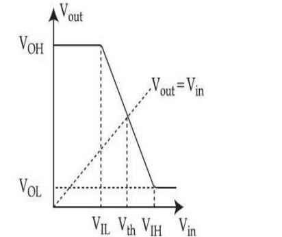
(B) VIL – VOL
(C) VOH – VIH
(D) VIH + VOH
(B) and (C) Only
A noise margin is always a difference between what one gate guarantees to produce and what the next will still accept, so the two margins are (B) and (C) — option 2.
\(NM_{L}=V_{IL}-V_{OL},\qquad NM_{H}=V_{OH}-V_{IH}\)
What the four voltages mean.
| Symbol | Meaning | Belongs to |
|---|---|---|
| VOL | Highest voltage the driver produces for a logic 0 | Output of gate 1 |
| VIL | Highest voltage the receiver still reads as 0 | Input of gate 2 |
| VIH | Lowest voltage the receiver still reads as 1 | Input of gate 2 |
| VOH | Lowest voltage the driver produces for a logic 1 | Output of gate 1 |
Reading the low margin. The driver's 0 sits at or below \(V_{OL}\), and the receiver accepts anything up to \(V_{IL}\) as a 0. The gap between them, \(V_{IL}-V_{OL}\), is how much noise can be added to a low signal before it is misread — statement (B).
Reading the high margin. Symmetrically, the driver's 1 is at least \(V_{OH}\) and the receiver accepts anything down to \(V_{IH}\), so noise of up to \(V_{OH}-V_{IH}\) can be subtracted — statement (C).
Why the sums in (A) and (D) are impossible. Adding two voltages that lie on the same scale produces a number larger than the supply rail, which cannot be a margin: a margin must be smaller than the logic swing, and it must vanish when the transfer curve degrades. Only a difference has those properties. (A) also adds two input thresholds, which never combine, and (D) mixes an input threshold with an output level in a sum rather than a difference.
Where VIL and VIH come from on the curve. They are defined as the points where the transfer characteristic has a slope of exactly −1. Below \(V_{IL}\) and above \(V_{IH}\) the gain magnitude is less than 1, so a disturbance at the input emerges attenuated — noise dies away as it passes down a chain of gates. Between them the gain exceeds 1 and noise would be amplified, which is why that band is excluded from both margins.
Why NMOS is the weaker case. Its pull-up is a load device that never turns off, so \(V_{OL}\) cannot reach ground and the low margin is squeezed. CMOS drives its output rail to rail, giving nearly equal and much larger margins — one of the main reasons it displaced NMOS.
Hence, the noise margins are (B) and (C).
Similar Questions
CMOS inverter has following minimum number of region of operation.
Consider a resistive load inverter with VDD = 5V, K'n=20 $\mu$A/V2, VTO = 0.7 V, RL= 500 k$k\Omega$ and \(\frac{W}{L}\) = 3. Value of critical voltage VOH is:
CMOS logic gates are preferred over TTL logic as :
(a) CMOS has lower power dissipation and high fan out
(b) Needs no protection circuitry
(c) Propagation delay is small as compared to TTL
(d) High noise margin for higher values of VDD
Out of the above, the following is true :
Important Questions from Unipolar Logic Families - Teaching
CMOS inverter has following minimum number of region of operation.
Consider a resistive load inverter with VDD = 5V, K'n=20 $\mu$A/V2, VTO = 0.7 V, RL= 500 k$k\Omega$ and \(\frac{W}{L}\) = 3. Value of critical voltage VOH is:
CMOS logic gates are preferred over TTL logic as :
(a) CMOS has lower power dissipation and high fan out
(b) Needs no protection circuitry
(c) Propagation delay is small as compared to TTL
(d) High noise margin for higher values of VDD
Out of the above, the following is true :



