
CMOS logic gates are preferred over TTL logic as : (a) CMOS has lower power dissipation and high fan out (b) Needs no protection circuitry (c) Propagation delay is small as compared to TTL (d) High noise margin for higher values of VDD Out of the above, the following is true :
(a) and (d)
Statement (a) — correct on both counts.
Lower power. In a CMOS inverter one of the two transistors is always off, so in the static state no path exists from VDD to ground and the only current is leakage — nanowatts per gate, against milliwatts for TTL. Power is consumed essentially only while switching:
\(P=C_LV_{DD}^{2}f\)
High fan-out. A CMOS gate input is an insulated gate, so it draws no DC current at all — only a small capacitance. Fan-out is therefore around 50, against TTL's 10, and is limited by speed rather than by loading.
Statement (d) — correct. CMOS switches at roughly VDD/2 and swings rail to rail, so the noise margin is about
\(NM\approx0.45\,V_{DD}\)
At 5 V that is about 2.25 V, and raising VDD to 15 V raises it proportionally — far beyond TTL's fixed 0.4 V, which is set by the silicon junction voltages and cannot be improved by raising the supply.
Statement (b) — wrong, and it is the exact opposite of the truth. The thin gate oxide of a MOS transistor breaks down at only a few tens of volts, and static electricity easily exceeds that. CMOS therefore requires on-chip ESD protection diodes on every input, and careful handling — earthed wrist straps, conductive foam — in the workshop. This vulnerability is one of CMOS's few genuine disadvantages relative to TTL.
Statement (c) — wrong for the era this question describes. Classic CMOS is slower than TTL: the 4000 series has a propagation delay of 40–100 ns at 5 V against 10 ns for standard TTL, because the p-channel devices have lower mobility and the gate must charge capacitive loads through a relatively high on-resistance. Later families such as HC and AC closed the gap, but CMOS was never preferred over TTL for its speed.
Assemble. (a) and (d) are correct, which is option 3.
| CMOS | TTL | |
|---|---|---|
| Static power/gate | ≈ 10 nW | ≈ 10 mW |
| Fan-out | ≈ 50 | 10 |
| Noise margin | 0.45 VDD | 0.4 V |
| Propagation delay | slower (4000 series) | faster |
| ESD protection | essential | not needed |
Hence, the true statements are (a) and (d).
Similar Questions
The typical voltage transfer characteristics of a realistic nmos invertor are shown in fig. The noise margin for low signal and high signal levels are :
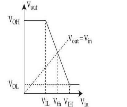
(A) VIL + VIH
(B) VIL – VOL
(C) VOH – VIH
(D) VIH + VOHChoose the most appropriate answer from the options given below :
CMOS inverter has following minimum number of region of operation.
Consider a resistive load inverter with VDD = 5V, K'n=20 $\mu$A/V2, VTO = 0.7 V, RL= 500 k$k\Omega$ and \(\frac{W}{L}\) = 3. Value of critical voltage VOH is:
Important Questions from Unipolar Logic Families - Teaching
The typical voltage transfer characteristics of a realistic nmos invertor are shown in fig. The noise margin for low signal and high signal levels are :
(A) VIL + VIH
(B) VIL – VOL
(C) VOH – VIH
(D) VIH + VOHChoose the most appropriate answer from the options given below :
CMOS inverter has following minimum number of region of operation.
Consider a resistive load inverter with VDD = 5V, K'n=20 $\mu$A/V2, VTO = 0.7 V, RL= 500 k$k\Omega$ and \(\frac{W}{L}\) = 3. Value of critical voltage VOH is:



