
Consider a resistive load inverter with VDD = 5V, K'n=20 $\mu$A/V2, VTO = 0.7 V, RL= 500 k$k\Omega$ and \(\frac{W}{L}\) = 3. Value of critical voltage VOH is:
5V
The circuit. A resistive-load inverter is an nMOS driver transistor whose drain is tied to VDD through a load resistor RL, with the output taken at the drain.
What VOH means. VOH is the output-high level, i.e. the output voltage when the input is LOW.
Reason it out. For the output to be high, the input must be below the threshold:
\(V_{in} \lt V_{TO} = 0.7\ \text{V} \Rightarrow \text{the driver transistor is in CUT-OFF}\)
A cut-off transistor conducts no drain current, so \(I_D = 0\) and there is no drop across the load resistor:
\(V_{OH} = V_{DD} - I_D R_L = V_{DD} - 0 = 5\ \text{V}\)
Note which data are red herrings. K'n, W/L and RL play no part in VOH at all — they matter only for the output-low level, where the transistor is ON in the linear region and VOL is set by the ratio of the driver's on-resistance to RL:
\(\dfrac{V_{DD}-V_{OL}}{R_L}=K'_n\dfrac{W}{L}\left[(V_{OH}-V_{TO})V_{OL}-\dfrac{V_{OL}^{2}}{2}\right]\)
which is where the small value 0.147 V among the options comes from. Recognising which critical voltage is being asked for is the whole trick of this question.
The wider point. Because a resistive (or depletion-load) nMOS inverter draws steady current whenever the output is LOW, it burns static power in that state — the flaw CMOS removes by replacing the resistor with a PMOS transistor that turns OFF when the NMOS turns ON. In CMOS the same reasoning still gives a full-rail VOH = VDD, but now with zero static current in both states.
Hence, VOH = 5 V.
Similar Questions
The typical voltage transfer characteristics of a realistic nmos invertor are shown in fig. The noise margin for low signal and high signal levels are :
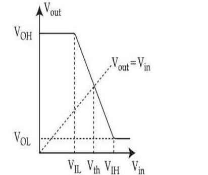
(A) VIL + VIH
(B) VIL – VOL
(C) VOH – VIH
(D) VIH + VOHChoose the most appropriate answer from the options given below :
CMOS inverter has following minimum number of region of operation.
CMOS logic gates are preferred over TTL logic as :
(a) CMOS has lower power dissipation and high fan out
(b) Needs no protection circuitry
(c) Propagation delay is small as compared to TTL
(d) High noise margin for higher values of VDD
Out of the above, the following is true :
Important Questions from Unipolar Logic Families - Teaching
The typical voltage transfer characteristics of a realistic nmos invertor are shown in fig. The noise margin for low signal and high signal levels are :
(A) VIL + VIH
(B) VIL – VOL
(C) VOH – VIH
(D) VIH + VOHChoose the most appropriate answer from the options given below :
CMOS inverter has following minimum number of region of operation.
CMOS logic gates are preferred over TTL logic as :
(a) CMOS has lower power dissipation and high fan out
(b) Needs no protection circuitry
(c) Propagation delay is small as compared to TTL
(d) High noise margin for higher values of VDD
Out of the above, the following is true :



