
CMOS inverter has following minimum number of region of operation.
5
What is being counted. The question asks how many distinct regions appear in the voltage transfer characteristic (VTC) of a CMOS inverter as the input Vin is swept from 0 to VDD. A region is defined by the pair of operating states of the two transistors.
The structure. A CMOS inverter is a PMOS pull-up (source at VDD) stacked on an NMOS pull-down (source at ground), gates tied together to Vin and drains tied together to Vout. The NMOS conducts when \(V_{in} \gt V_{Tn}\); the PMOS conducts when \(V_{in} \lt V_{DD} - |V_{Tp}|\). Each conducting transistor is in the linear (triode) region when its VDS is small and in saturation when VDS is large.
Sweeping the input gives five regions:
| Region | Input range | NMOS | PMOS | Output |
|---|---|---|---|---|
| 1 | \(V_{in} \lt V_{Tn}\) | Cut-off | Linear | VOH = VDD |
| 2 | low, above VTn | Saturation | Linear | falling slowly |
| 3 | near VDD/2 | Saturation | Saturation | steep transition |
| 4 | high, below VDD−|VTp| | Linear | Saturation | falling slowly |
| 5 | \(V_{in} \gt V_{DD} - |V_{Tp}|\) | Linear | Cut-off | VOL = 0 |
Why this matters in practice. In regions 1 and 5 exactly one transistor is OFF, so no d.c. path exists between VDD and ground and the static power is essentially zero (only leakage) — this is the reason CMOS dominates digital design. Current flows from supply to ground only in the middle regions, with a peak in region 3, where both devices are saturated. Region 3 also contains the switching threshold VM, the point where \(V_{out} = V_{in}\) and the gain is highest.
Counting the distinct operating-state combinations gives 1 + 1 + 1 + 1 + 1 = 5.
Hence, the CMOS inverter has a minimum of 5 regions of operation.
Similar Questions
The typical voltage transfer characteristics of a realistic nmos invertor are shown in fig. The noise margin for low signal and high signal levels are :
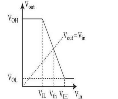
(A) VIL + VIH
(B) VIL – VOL
(C) VOH – VIH
(D) VIH + VOHChoose the most appropriate answer from the options given below :
Consider a resistive load inverter with VDD = 5V, K'n=20 $\mu$A/V2, VTO = 0.7 V, RL= 500 k$k\Omega$ and \(\frac{W}{L}\) = 3. Value of critical voltage VOH is:
CMOS logic gates are preferred over TTL logic as :
(a) CMOS has lower power dissipation and high fan out
(b) Needs no protection circuitry
(c) Propagation delay is small as compared to TTL
(d) High noise margin for higher values of VDD
Out of the above, the following is true :
Important Questions from Unipolar Logic Families - Teaching
The typical voltage transfer characteristics of a realistic nmos invertor are shown in fig. The noise margin for low signal and high signal levels are :
(A) VIL + VIH
(B) VIL – VOL
(C) VOH – VIH
(D) VIH + VOHChoose the most appropriate answer from the options given below :
Consider a resistive load inverter with VDD = 5V, K'n=20 $\mu$A/V2, VTO = 0.7 V, RL= 500 k$k\Omega$ and \(\frac{W}{L}\) = 3. Value of critical voltage VOH is:
CMOS logic gates are preferred over TTL logic as :
(a) CMOS has lower power dissipation and high fan out
(b) Needs no protection circuitry
(c) Propagation delay is small as compared to TTL
(d) High noise margin for higher values of VDD
Out of the above, the following is true :



