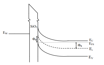
Match List I with List II Choose the correct answer from the options given below:LIST I LIST II A. When negative VG is applied to gate of MOS I. Depletion B. When zero-bias is applied to gate of MOS II. Surface Inversion C. When a small positive gate bias VG is applied to gate of MOS III. Accumulation D. When a higher positive gate VG is applied to gate of MOS IV. Neutral MOS
A-I, B-IV, C-III, D-II
The task is to match the conditions (List I) applied to the gate of a Metal-Oxide-Semiconductor (MOS) device with the associated effects (List II). Let's analyze and understand each condition and its effect on the MOS structure:
- When negative \(V_G\) is applied to gate of MOS:
- When a negative gate voltage is applied, it causes the holes (majority carriers in p-type substrate) to gather at the oxide interface, depleting the region of free electrons.
- This condition is known as Depletion.
- Therefore, A-I is the correct match.
- When zero-bias is applied to gate of MOS:
- In this scenario, there is no influence from the gate voltage on the MOS capacitor, so the charge carriers remain in their neutral state.
- This condition reflects a Neutral MOS.
- Thus, B-IV is the correct match.
- When a small positive gate bias \(V_G\) is applied to gate of MOS:
- A small positive voltage attracts electrons toward the oxide interface, causing an accumulation of negative charge at the surface.
- This is known as Accumulation.
- Hence, C-III is the correct match.
- When a higher positive gate \(V_G\) is applied to gate of MOS:
- A high positive gate voltage significantly attracts electrons to form a conductive channel at the surface, resulting in the strong inversion of the surface.
- This condition is termed as Surface Inversion.
- Thus, D-II is the correct match.
After considering the explanations above, the correct matching is:
- A-I
- B-IV
- C-III
- D-II
Hence, the correct answer is: A-I, B-IV, C-III, D-II.
Similar Questions
In a MOS structure the φm is the work function of metal and φs is the work function of semiconductor then the flat band voltage is :
In ideal MOS diode
(a) φms = 0
(b) \(\phi_m+\varphi_B=\chi+\dfrac{E_g}{2q}\)
(c) \(\phi_m-\varphi_B-\chi=E_g\)
(d) \(\varphi_B+\chi=\dfrac{E_g}{2}\)
Out of the above which are correct ?
Important Questions from MOS Capacitor
BiCMOS technology is integration of
In a MOS structure the φm is the work function of metal and φs is the work function of semiconductor then the flat band voltage is :
In ideal MOS diode
(a) φms = 0
(b) \(\phi_m+\varphi_B=\chi+\dfrac{E_g}{2q}\)
(c) \(\phi_m-\varphi_B-\chi=E_g\)
(d) \(\varphi_B+\chi=\dfrac{E_g}{2}\)
Out of the above which are correct ?
- Consider a MOS capacitor made with p-type silicon. It has an oxide thickness of 100 nm, a fixed positive oxide charge of $10^{-8}$ C/cm$^2$ at the oxide-silicon interface, and a metal work function of 4.6 eV. Assume that the relative permittivity of the oxide is 4 and the absolute permittivity of free space is $8.85 \times 10^{-14}$ F/cm. If the flatband voltage is 0 V, the work function of the p-type silicon (in eV, rounded off to two decimal places) is ________.
The figure shows the band diagram of a Metal Oxide Semiconductor (MOS). The surface region of this MOS is in