BiCMOS technology is integration of
BJT and CMOS
BiCMOS Technology: An Overview
BiCMOS technology represents a sophisticated method of integrating different types of transistors onto a single integrated circuit (IC) chip. The term BiCMOS itself is an acronym formed from its two core components: Bipolar Junction Transistors (BJTs) and CMOS (Complementary Metal-Oxide-Semiconductor) technology.
This integration aims to harness the distinct advantages of both BJT and CMOS transistors, overcoming the limitations of using either technology exclusively for certain applications.
BiCMos Integration Explained
Let's break down the components of BiCMOS technology:
- BJT (Bipolar Junction Transistor): BJTs are known for their high current driving capability, high transconductance, and excellent high-frequency performance. They are typically used in analog circuits, high-speed switching applications, and for output drivers that require significant current. However, BJTs consume more power in static operation and have a lower input impedance compared to MOSFETs.
- CMOS (Complementary Metal-Oxide-Semiconductor): CMOS technology is renowned for its extremely low static power consumption, high input impedance, and good noise immunity. It is the dominant technology for digital integrated circuits due to its efficient design for logic gates. However, CMOS circuits typically have lower current drive capabilities and are slower than BJT circuits at very high frequencies when driving large loads.
Advantages of BiCMOS Technology
By combining BJTs and CMOS on the same chip, BiCMOS technology achieves a blend of their strengths, leading to circuits that exhibit:
- High Speed: Leveraging the fast switching characteristics of BJTs.
- Low Power Consumption: Benefiting from the low static power dissipation of CMOS.
- High Input Impedance: A characteristic of CMOS circuits.
- High Current Drive Capability: Provided by BJTs, which is crucial for driving large capacitive loads.
- Improved Noise Margins: Leading to more robust circuit operation.
This hybrid approach makes BiCMOS technology particularly suitable for applications where both high speed/current drive and low power consumption are critical. Examples include high-speed microprocessors, memory interfaces, data converters (ADCs/DACs), and high-performance analog circuits.
Therefore, BiCMOS technology is essentially the integration of BJT and CMOS transistors.
Important Questions from MOS Capacitor
In a MOS structure the φm is the work function of metal and φs is the work function of semiconductor then the flat band voltage is :
Match List I with List II
LIST I LIST II A. When negative VG is applied to gate of MOS I. Depletion B. When zero-bias is applied to gate of MOS II. Surface Inversion C. When a small positive gate bias VG is applied to gate of MOS III. Accumulation D. When a higher positive gate VG is applied to gate of MOS IV. Neutral MOS Choose the correct answer from the options given below:
In ideal MOS diode
(a) φms = 0
(b) \(\phi_m+\varphi_B=\chi+\dfrac{E_g}{2q}\)
(c) \(\phi_m-\varphi_B-\chi=E_g\)
(d) \(\varphi_B+\chi=\dfrac{E_g}{2}\)
Out of the above which are correct ?
- Consider a MOS capacitor made with p-type silicon. It has an oxide thickness of 100 nm, a fixed positive oxide charge of $10^{-8}$ C/cm$^2$ at the oxide-silicon interface, and a metal work function of 4.6 eV. Assume that the relative permittivity of the oxide is 4 and the absolute permittivity of free space is $8.85 \times 10^{-14}$ F/cm. If the flatband voltage is 0 V, the work function of the p-type silicon (in eV, rounded off to two decimal places) is ________.
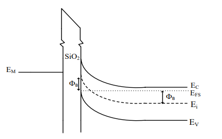
The figure shows the band diagram of a Metal Oxide Semiconductor (MOS). The surface region of this MOS is in