MOS Capacitor Work Function Calculation
This solution details the calculation of the work function of p-type silicon in a MOS capacitor, considering given parameters like oxide thickness, fixed oxide charge, and metal work function.
MOS Capacitor Given Parameters
| Parameter | Symbol | Value | Units |
| Oxide thickness | $t_{ox}$ | 100 | nm |
| Fixed positive oxide charge | $Q_{f}$ | $10^{-8}$ | C/cm$^2$ |
| Metal work function | $\Phi_{m}$ | 4.6 | eV |
| Relative permittivity of oxide | $\epsilon_{r}$ | 4 | - |
| Absolute permittivity of free space | $\epsilon_{0}$ | $8.85 \times 10^{-14}$ | F/cm |
| Flatband voltage | $V_{FB}$ | 0 | V |
Capacitor Calculations
First, the oxide capacitance per unit area ($C_{ox}$) needs to be calculated. Ensure all units are consistent.
- Convert oxide thickness to cm: $t_{ox} = 100 \text{ nm} = 100 \times 10^{-7} \text{ cm} = 1 \times 10^{-5} \text{ cm}$
- Calculate the permittivity of the oxide ($\epsilon_{ox}$): $\epsilon_{ox} = \epsilon_{r} \times \epsilon_{0} = 4 \times (8.85 \times 10^{-14} \text{ F/cm}) = 3.54 \times 10^{-13} \text{ F/cm}$
- Calculate the oxide capacitance ($C_{ox}$): $C_{ox} = \frac{\epsilon_{ox}}{t_{ox}} = \frac{3.54 \times 10^{-13} \text{ F/cm}}{1 \times 10^{-5} \text{ cm}} = 3.54 \times 10^{-8} \text{ F/cm}^2$
The flatband voltage ($V_{FB}$) for a MOS capacitor is given by the formula:
$V_{FB} = \Phi_{m} - \Phi_{s} - \frac{Q_{f}}{C_{ox}}$Where $\Phi_{m}$ is the metal work function and $\Phi_{s}$ is the semiconductor work function.
Rearrange the formula to solve for the work function of the p-type silicon ($\Phi_{s}$):
$\Phi_{s} = \Phi_{m} - V_{FB} - \frac{Q_{f}}{C_{ox}}$Substitute the given values:
- $V_{FB} = 0$ V
- $\Phi_{m} = 4.6$ eV
- $Q_{f} = 10^{-8}$ C/cm$^2$
- $C_{ox} = 3.54 \times 10^{-8}$ F/cm$^2$
Calculate the term $\frac{Q_{f}}{C_{ox}}$:
$\frac{Q_{f}}{C_{ox}} = \frac{10^{-8} \text{ C/cm}^2}{3.54 \times 10^{-8} \text{ F/cm}^2} \approx 0.2825 \text{ V}$Now, calculate $\Phi_{s}$:
$\Phi_{s} = 4.6 \text{ eV} - 0 \text{ V} - 0.2825 \text{ V}$ $\Phi_{s} \approx 4.3175 \text{ eV}$Final Work Function Result
Rounding the result to two decimal places as required:
$\Phi_{s} \approx 4.32 \text{ eV}$Important Questions from MOS Capacitor
BiCMOS technology is integration of
In a MOS structure the φm is the work function of metal and φs is the work function of semiconductor then the flat band voltage is :
Match List I with List II
LIST I LIST II A. When negative VG is applied to gate of MOS I. Depletion B. When zero-bias is applied to gate of MOS II. Surface Inversion C. When a small positive gate bias VG is applied to gate of MOS III. Accumulation D. When a higher positive gate VG is applied to gate of MOS IV. Neutral MOS Choose the correct answer from the options given below:
In ideal MOS diode
(a) φms = 0
(b) \(\phi_m+\varphi_B=\chi+\dfrac{E_g}{2q}\)
(c) \(\phi_m-\varphi_B-\chi=E_g\)
(d) \(\varphi_B+\chi=\dfrac{E_g}{2}\)
Out of the above which are correct ?
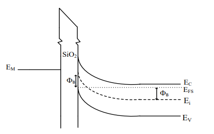
The figure shows the band diagram of a Metal Oxide Semiconductor (MOS). The surface region of this MOS is in