
The figure shows the band diagram of a Metal Oxide Semiconductor (MOS). The surface region of this MOS is in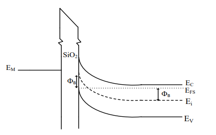
The given question pertains to the analysis of a Metal Oxide Semiconductor (MOS) device and its band diagram. To determine the condition of the surface region, we need to understand band bending and the position of the Fermi level within the semiconductor region. Let's analyze the band diagram shown in the image:
- The band diagram shows the energy levels within the semiconductor and consists of the conduction band edge (\(E_C\)), the valence band edge (\(E_V\)), and the intrinsic energy level (\(E_i\)).
- The Fermi level at the surface (\(E_{FS}\)) is significantly closer to the conduction band edge compared to the intrinsic energy level. This indicates an increase in electron concentration near the surface.
- Such a condition is commonly referred to as "inversion." In this state, the electron concentration exceeds the hole concentration at the surface, effectively converting the type of semiconductor from p-type to n-type at the surface.
- The characteristic feature of inversion is the bending of the bands such that the Fermi level appears closer to the conduction band at the surface, as seen in the diagram. This confirms that the surface is indeed in inversion mode.
Conclusion: Based on the analysis of the band diagram where the Fermi level is closer to the conduction band at the surface, the surface region of this MOS device is in the condition of inversion.
Important Questions from MOS Capacitor
BiCMOS technology is integration of
In a MOS structure the φm is the work function of metal and φs is the work function of semiconductor then the flat band voltage is :
Match List I with List II
LIST I LIST II A. When negative VG is applied to gate of MOS I. Depletion B. When zero-bias is applied to gate of MOS II. Surface Inversion C. When a small positive gate bias VG is applied to gate of MOS III. Accumulation D. When a higher positive gate VG is applied to gate of MOS IV. Neutral MOS Choose the correct answer from the options given below:
In ideal MOS diode
(a) φms = 0
(b) \(\phi_m+\varphi_B=\chi+\dfrac{E_g}{2q}\)
(c) \(\phi_m-\varphi_B-\chi=E_g\)
(d) \(\varphi_B+\chi=\dfrac{E_g}{2}\)
Out of the above which are correct ?
- Consider a MOS capacitor made with p-type silicon. It has an oxide thickness of 100 nm, a fixed positive oxide charge of $10^{-8}$ C/cm$^2$ at the oxide-silicon interface, and a metal work function of 4.6 eV. Assume that the relative permittivity of the oxide is 4 and the absolute permittivity of free space is $8.85 \times 10^{-14}$ F/cm. If the flatband voltage is 0 V, the work function of the p-type silicon (in eV, rounded off to two decimal places) is ________.


