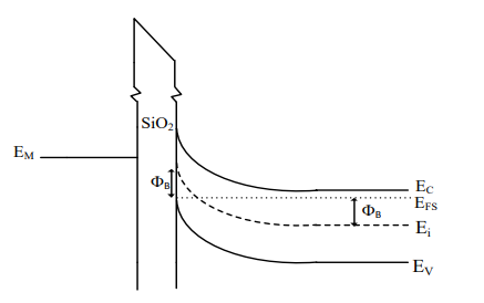
In a MOS structure the φm is the work function of metal and φs is the work function of semiconductor then the flat band voltage is :
\(\phi_{m}-\phi_{s}\)
The flat-band voltage is the work-function difference, option 3:
\(V_{FB}=\phi_{ms}=\phi_{m}-\phi_{s}\)
What flat band means, and why a difference appears. Bring a metal and a semiconductor into contact through an oxide. Their Fermi levels must align in equilibrium, and if their work functions differ the semiconductor's bands must bend near the surface to accommodate the mismatch. The flat-band voltage is the gate voltage that has to be applied to undo that bending — to make the energy bands run flat right up to the oxide interface.
The voltage needed is precisely the mismatch that caused the bending, so it is the difference of the two work functions and nothing else. A sum, as in options 1 and 2, would be an absolute energy rather than a mismatch, and would not vanish when the two materials are matched — yet a structure with \(\phi_{m}=\phi_{s}\) plainly needs no applied voltage to sit flat. That single test disposes of every option except 3.
| Case | φms | Surface at zero bias |
|---|---|---|
| φm = φs | 0 | Already flat |
| φm < φs | Negative | Bands bent down — surface tends to n-type |
| φm > φs | Positive | Bands bent up — surface tends to p-type |
Why it matters. The flat-band voltage is the reference point from which every other MOS voltage is measured, and it shifts the threshold directly:
\(V_{T}=V_{FB}+2\phi_{F}+\dfrac{\sqrt{2q\varepsilon_{s}N_{A}\left(2\phi_{F}\right)}}{C_{ox}}\)
which is why the gate material is chosen for its work function. Aluminium gates gave one value; the switch to heavily doped polysilicon allowed the gate's own doping to set \(\phi_{m}\), so n+ poly could be used for NMOS and p+ poly for PMOS, giving each the threshold it needs. Metal-gate work-function engineering in modern high-k processes does the same job with different materials.
The complete expression adds the effect of charge trapped in and near the oxide:
\(V_{FB}=\phi_{ms}-\dfrac{Q_{ox}}{C_{ox}}\)
Sodium contamination early in the industry's history produced a mobile \(Q_{ox}\) that made thresholds drift with time and bias — the problem whose solution made stable MOS manufacturing possible.
Hence, the flat band voltage is φm − φs.
Similar Questions
Match List I with List II
LIST I LIST II A. When negative VG is applied to gate of MOS I. Depletion B. When zero-bias is applied to gate of MOS II. Surface Inversion C. When a small positive gate bias VG is applied to gate of MOS III. Accumulation D. When a higher positive gate VG is applied to gate of MOS IV. Neutral MOS Choose the correct answer from the options given below:
In ideal MOS diode
(a) φms = 0
(b) \(\phi_m+\varphi_B=\chi+\dfrac{E_g}{2q}\)
(c) \(\phi_m-\varphi_B-\chi=E_g\)
(d) \(\varphi_B+\chi=\dfrac{E_g}{2}\)
Out of the above which are correct ?
Important Questions from MOS Capacitor
BiCMOS technology is integration of
Match List I with List II
LIST I LIST II A. When negative VG is applied to gate of MOS I. Depletion B. When zero-bias is applied to gate of MOS II. Surface Inversion C. When a small positive gate bias VG is applied to gate of MOS III. Accumulation D. When a higher positive gate VG is applied to gate of MOS IV. Neutral MOS Choose the correct answer from the options given below:
In ideal MOS diode
(a) φms = 0
(b) \(\phi_m+\varphi_B=\chi+\dfrac{E_g}{2q}\)
(c) \(\phi_m-\varphi_B-\chi=E_g\)
(d) \(\varphi_B+\chi=\dfrac{E_g}{2}\)
Out of the above which are correct ?
- Consider a MOS capacitor made with p-type silicon. It has an oxide thickness of 100 nm, a fixed positive oxide charge of $10^{-8}$ C/cm$^2$ at the oxide-silicon interface, and a metal work function of 4.6 eV. Assume that the relative permittivity of the oxide is 4 and the absolute permittivity of free space is $8.85 \times 10^{-14}$ F/cm. If the flatband voltage is 0 V, the work function of the p-type silicon (in eV, rounded off to two decimal places) is ________.
The figure shows the band diagram of a Metal Oxide Semiconductor (MOS). The surface region of this MOS is in