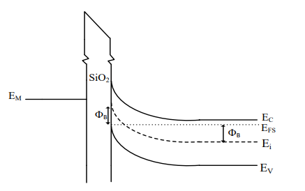
In ideal MOS diode (a) φms = 0 (b) \(\phi_m+\varphi_B=\chi+\dfrac{E_g}{2q}\) (c) \(\phi_m-\varphi_B-\chi=E_g\) (d) \(\varphi_B+\chi=\dfrac{E_g}{2}\) Out of the above which are correct ?
(a) and (b) are correct
What "ideal" means for a MOS diode. The ideal MOS structure is defined by the condition that, with zero gate bias, the energy bands in the semiconductor are flat right up to the oxide — there is no built-in band bending. That requires the metal work function to equal the semiconductor work function, i.e. the work-function difference vanishes:
\(\phi_{ms}=\phi_m-\phi_s=0\)
So statement (a) is correct — it is the definition itself.
Writing the semiconductor work function out. Measured from the vacuum level, the semiconductor work function is the electron affinity plus the distance from the conduction band edge down to the Fermi level. Expressed through the mid-gap and the bulk potential φB:
\(\phi_s=\chi+\dfrac{E_g}{2q}\mp\varphi_B\)
the sign depending on whether the substrate is p-type or n-type. Setting \(\phi_m=\phi_s\) and rearranging gives
\(\phi_m+\varphi_B=\chi+\dfrac{E_g}{2q}\)
which is statement (b) — the same flat-band condition written out in terms of measurable material parameters. So (a) and (b) say the same thing in two ways, which is exactly why they belong together.
Why (c) and (d) fail. Both are dimensionally inconsistent. The terms φm, φB and χ are all potentials measured in volts, whereas Eg is an energy in electron-volts. Statement (c) equates a combination of volts to Eg without the dividing q, and (d) equates volts to Eg/2 — again missing the charge. The correct form always carries Eg/2q, as in (b). Checking units is the fastest way to reject options in questions of this type.
Why the ideal case matters. Real structures never satisfy it: the work functions differ and the oxide carries fixed, mobile and interface-trapped charge, so a non-zero flat-band voltage is needed to restore flat bands:
\(V_{FB}=\phi_{ms}-\dfrac{Q_{ox}}{C_{ox}}\)
and VFB shifts the whole C–V curve and hence the MOSFET threshold voltage.
Hence, the correct statements are (a) and (b).
Similar Questions
In a MOS structure the φm is the work function of metal and φs is the work function of semiconductor then the flat band voltage is :
Match List I with List II
LIST I LIST II A. When negative VG is applied to gate of MOS I. Depletion B. When zero-bias is applied to gate of MOS II. Surface Inversion C. When a small positive gate bias VG is applied to gate of MOS III. Accumulation D. When a higher positive gate VG is applied to gate of MOS IV. Neutral MOS Choose the correct answer from the options given below:
Important Questions from MOS Capacitor
BiCMOS technology is integration of
In a MOS structure the φm is the work function of metal and φs is the work function of semiconductor then the flat band voltage is :
Match List I with List II
LIST I LIST II A. When negative VG is applied to gate of MOS I. Depletion B. When zero-bias is applied to gate of MOS II. Surface Inversion C. When a small positive gate bias VG is applied to gate of MOS III. Accumulation D. When a higher positive gate VG is applied to gate of MOS IV. Neutral MOS Choose the correct answer from the options given below:
- Consider a MOS capacitor made with p-type silicon. It has an oxide thickness of 100 nm, a fixed positive oxide charge of $10^{-8}$ C/cm$^2$ at the oxide-silicon interface, and a metal work function of 4.6 eV. Assume that the relative permittivity of the oxide is 4 and the absolute permittivity of free space is $8.85 \times 10^{-14}$ F/cm. If the flatband voltage is 0 V, the work function of the p-type silicon (in eV, rounded off to two decimal places) is ________.
The figure shows the band diagram of a Metal Oxide Semiconductor (MOS). The surface region of this MOS is in