
In the following circuit, for the given inputs V1 and V2, the correct option for output V0 is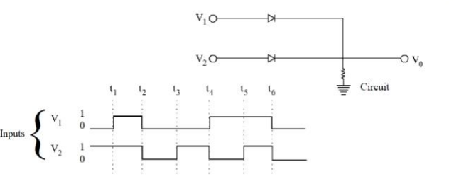

Identify the circuit. Both diodes have their anodes driven by the two inputs V1 and V2, their cathodes are tied together at the output node V0, and a resistor returns that node to ground. This is the classic diode-logic (DL) positive-logic OR gate.
How a diode behaves here. A diode conducts only when its anode is more positive than its cathode by about 0.7 V (silicon). Otherwise it is reverse biased and behaves as an open circuit. In this circuit the cathodes sit at V0, so a diode turns ON only when its own input is the highest voltage present.
Case-by-case analysis (positive logic: HIGH = 1, LOW = 0).
1. V1 = 0, V2 = 0 — neither diode is forward biased, no current flows, and the resistor holds the output at ground. V0 = 0.
2. V1 = 1, V2 = 0 — the upper diode conducts and pulls the output up to \(V_0 = V_1 - 0.7\ \text{V}\), i.e. logic HIGH. The lower diode now has 0 V on its anode and a positive cathode, so it is reverse biased and isolates the LOW input.
3. V1 = 0, V2 = 1 — by symmetry the lower diode conducts and V0 is HIGH.
4. V1 = 1, V2 = 1 — the diode with the larger input conducts; the output follows the larger of the two inputs and is HIGH.
Truth table. The four cases give 0, 1, 1, 1 — exactly the OR function:
\(V_0 = V_1 + V_2 \quad (\text{logical OR})\)
Building the output waveform. Because the gate is an OR, the output waveform is simply the union of the HIGH intervals of the two inputs: mark every instant at which either input is HIGH, and the output is HIGH there; the output is LOW only in intervals where both inputs are simultaneously LOW. Sketching that union over the given input timing reproduces the waveform of option 3.
Key idea to remember. The diode orientation decides the function: anodes to the inputs with a pull-down resistor gives an OR gate (output follows the highest input), whereas cathodes to the inputs with a pull-up resistor to +V gives an AND gate (output follows the lowest input). Also note that each stage loses one diode drop (~0.7 V), which is why diode logic cannot be cascaded indefinitely and why transistor logic families replaced it.
Hence, the output is the logical OR of the two inputs — HIGH wherever V1 or V2 is HIGH and LOW only when both are LOW — which is the third waveform.
Similar Questions
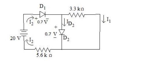
What current should flow through D2 diode? Consider the values given in circuit below.
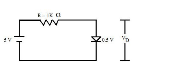
The diode used in fig. below has the threshold voltage of 0.5 V and a forward resistance of 4$\Omega$ Calculate the current flow ID through and the voltage drop VD across the diode.
Match the following lists :
List – I List – II a. Voltage doubler i. 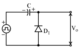
b. Halfwave rectifier ii. 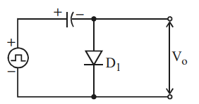
c. Positive clamping circuit iii. 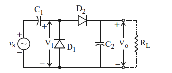
d. Negative clamping circuit iv. 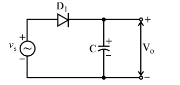
Codes :
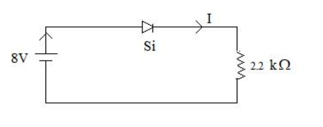
The value of current I flowing in the given circuit is:
Important Questions from Diodes and Its Applications - Teaching
What current should flow through D2 diode? Consider the values given in circuit below.
The diode used in fig. below has the threshold voltage of 0.5 V and a forward resistance of 4$\Omega$ Calculate the current flow ID through and the voltage drop VD across the diode.
Match the following lists :
List – I List – II a. Voltage doubler i. b. Halfwave rectifier ii. c. Positive clamping circuit iii. d. Negative clamping circuit iv. Codes :
- Assertion (A) : Clippers are networks that employ diodes to clip away a portion of an input signal without distorting the remaining part of the applied waveforms.
Reason (R) : In clipper circuit, the orientation of diode is very important and it decide the portion of the wave to be clipped. Clippers may be series or parallel type, depending upon the series/parallel connection of diode with the load. The value of current I flowing in the given circuit is:



