
Match the following : Codes :List - I List - II (figure in the original question) (a) n-channel Enhancement (Normally off) (i) 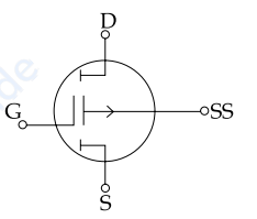
(b) p-channel Depletion MOSFET (Normally on) (ii) 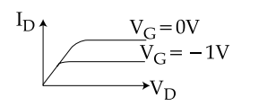
(c) n-channel FET (iii) 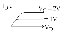
(d) p-channel Enhancement MOSFET (iv) 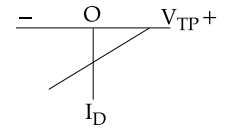
a-(iii), b-(iv), c-(ii), d-(i)
Read each figure for the one feature that identifies the device.
c → (ii), the n-channel FET (JFET). The curves are labelled VG = 0 V and VG = −1 V, with the larger current at zero gate voltage. A device that conducts fully at VGS = 0 and is turned down by a negative gate is a junction FET: its gate is a reverse-biased p-n junction, so the gate voltage can only ever deplete the channel, never enhance it.
a → (iii), the n-channel enhancement MOSFET. Here the curves carry VG = 2 V and 1 V, with more current at the higher positive gate voltage — and no curve at all for VG = 0. That is enhancement behaviour: the device is normally off, and a positive gate must be applied to invert the surface and create the channel.
\(I_D=\dfrac{\mu_nC_{ox}W}{2L}\left(V_{GS}-V_{TN}\right)^{2}, \qquad V_{GS} \gt V_{TN}\)
b → (iv), the p-channel depletion MOSFET. Two features fix it. The current axis points downward, the usual convention for the negative drain current of a p-channel device, and the threshold VTP sits on the positive side of the VGS axis. Crucially, the characteristic passes below the axis at VGS = 0 — there is already current with no gate bias, which is the signature of a depletion device ("normally on"). A physically implanted channel exists at zero bias and the gate depletes it.
d → (i), the p-channel enhancement MOSFET. The symbol settles it in two steps. The channel is drawn as three separate segments rather than a continuous line — the standard notation for an enhancement device, whose channel does not exist until it is induced. And the substrate arrow points away from the channel, toward the SS terminal, which denotes p-channel; an n-channel symbol has the arrow pointing inward.
Assemble. a-(iii), b-(iv), c-(ii), d-(i) — option 1.
The two rules that answer any question of this kind.
| Feature | Meaning |
|---|---|
| Continuous channel line | Depletion — normally on |
| Broken (segmented) channel line | Enhancement — normally off |
| Substrate arrow inward | n-channel |
| Substrate arrow outward | p-channel |
And on a transfer characteristic, the single question "is there current at VGS = 0?" separates depletion from enhancement immediately.
Hence, the correct matching is a-(iii), b-(iv), c-(ii), d-(i).
Similar Questions
A MOSFET differs from the JFET because
1. of the characteristics
2. the MOSFET has two gates
3. the JFET has p-n junctions
4. of the physical reduced size
Important Questions from Types of FET
The transconductance g mof a JFET is equal to:
\(\frac{ I _{ DSS }}{ V _{ P }}\left(1-\frac{ V _{ GS }}{ V _{ P }}\right)\)
The CMOS inverter can be used as an amplifier when:
In JFET, the Pinch‐off Voltage can be defined as:
In JFET, the current density in the x-direction is:
A. σ(x)E x
B. qN DμE x
C. \(\rm \frac{q}{2 \in_s}N_D\mu\)
D. \(\rm \frac{N_D\mu}{2 \in_s}\)
Choose the correct answer from the options given below:
Match List I with List II
List – I
List – II
JFET - Bias
Characteristic Equation
A.
Self - bias
I.
\(\rm I_D = \frac{V_{SS}-V_{GS}}{R_S}\)
B.
Voltage – divider bias
II.
\(\rm I_D = \frac{V_{EE}-V_{BE}}{R_E}\)
C.
Source bias
III.
V GS = -I DR S
D.
Current – source bias
IV.
\(\rm I_D = \frac{V_{G}-V_{GS}}{R_S}\)
Choose the correct answer from the options given below:



