Match List I with List II: Choose the correct answer from the options given below:List I List II (A) JFET (I) Two dimensional electron gas (B) MOSFET (II) Negative resistance device (C) Tunnel diode (III) Enhancement mode (D) HEMT (IV) Voltage controlled resistor
(A) - (IV), (B) - (III), (C) - (II), (D) - (I)
Understanding Semiconductor Devices and Their Characteristics
This question asks us to match different semiconductor devices with their specific characteristics or modes of operation. Let's analyze each device listed in List I and find its corresponding description in List II.
Analyzing List I and List II Matches
(A) JFET (Junction Field-Effect Transistor)
A JFET is a type of field-effect transistor that uses a gate-source pn junction to control the current flow through the channel. In its linear region, when the drain-source voltage is small, the channel behaves like a resistor whose resistance can be controlled by the gate-source voltage. Increasing the magnitude of the reverse gate voltage pinches off the channel, increasing its resistance. Therefore, a JFET acts as a voltage controlled resistor.
Match: JFET → Voltage controlled resistor
(B) MOSFET (Metal-Oxide-Semiconductor Field-Effect Transistor)
MOSFETs are widely used transistors with a gate separated from the channel by an insulating oxide layer. MOSFETs can operate in either depletion mode or enhancement mode. Enhancement mode MOSFETs are very common; they are normally off (no channel exists) and require a gate voltage of the correct polarity to create a conducting channel between the source and drain. This is the mode where the conductivity of the channel is "enhanced" by the gate voltage.
Match: MOSFET → Enhancement mode
(C) Tunnel Diode
A tunnel diode is a highly doped p-n junction diode that exhibits a quantum mechanical phenomenon called tunneling. Due to heavy doping, the depletion region is very narrow, allowing electrons to tunnel through the potential barrier. This tunneling effect leads to a unique current-voltage characteristic curve which shows a region where the current decreases as the voltage increases. This region is known as the negative differential resistance region. Thus, a tunnel diode is a negative resistance device.
Match: Tunnel diode → Negative resistance device
(D) HEMT (High Electron Mobility Transistor)
A HEMT is a type of field-effect transistor that incorporates a heterojunction between two semiconductor materials with different band gaps. This structure creates a thin layer at the interface where electrons can move very freely with high mobility. This layer is often referred to as a Two-Dimensional Electron Gas (2DEG). HEMTs are known for their high-speed switching capabilities, making them suitable for high-frequency applications.
Match: HEMT → Two dimensional electron gas
Summary of Matches
Based on our analysis, the correct matches are:
- (A) JFET - (IV) Voltage controlled resistor
- (B) MOSFET - (III) Enhancement mode
- (C) Tunnel diode - (II) Negative resistance device
- (D) HEMT - (I) Two dimensional electron gas
Let's present this in a table format for clarity.
| List I (Device) | List II (Characteristic) | Match |
|---|---|---|
| (A) JFET | (I) Two dimensional electron gas | (A) → (IV) |
| (B) MOSFET | (II) Negative resistance device | (B) → (III) |
| (C) Tunnel diode | (III) Enhancement mode | (C) → (II) |
| (D) HEMT | (IV) Voltage controlled resistor | (D) → (I) |
Conclusion
Comparing our matches with the given options, the set of matches (A) - (IV), (B) - (III), (C) - (II), (D) - (I) correctly aligns the semiconductor devices with their respective characteristics.
Revision Table: Semiconductor Device Characteristics
| Device | Key Characteristic | Notes |
|---|---|---|
| JFET | Voltage controlled resistor | Gate-source voltage controls channel conductivity. |
| MOSFET | Enhancement mode | Channel conductivity increases with gate voltage (requires gate voltage to form channel). |
| Tunnel Diode | Negative resistance device | Current decreases as voltage increases over a specific range due to quantum tunneling. |
| HEMT | Two dimensional electron gas (2DEG) | Utilizes a heterojunction to create a high mobility electron layer. |
Additional Information: Semiconductor Device Fundamentals
Understanding these devices is crucial in electronics. Here's a little more depth:
- JFET Operation: The gate voltage creates a depletion region that modulates the width of the conductive channel. It's a voltage-controlled current source in saturation but acts as a voltage-controlled resistor in the triode (linear) region.
- MOSFET Modes: Besides enhancement mode, MOSFETs also have depletion mode, where a channel exists at zero gate voltage, and the gate voltage depletes or reduces its conductivity. MOSFETs are widely used in digital circuits due to their low power consumption and scalability.
- Tunnel Diode Applications: The negative resistance property of tunnel diodes makes them useful in high-frequency oscillators and switching circuits.
- HEMT Technology: The 2DEG in HEMTs offers significantly higher electron mobility compared to conventional transistors, allowing them to operate at much higher frequencies, making them suitable for applications like satellite communications and radar systems.
Important Questions from Types of FET
A MOSFET differs from the JFET because
1. of the characteristics
2. the MOSFET has two gates
3. the JFET has p-n junctions
4. of the physical reduced size
Match the following :
List - I List - II (figure in the original question) (a) n-channel Enhancement (Normally off) (i) 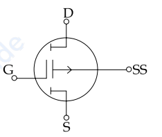
(b) p-channel Depletion MOSFET (Normally on) (ii) 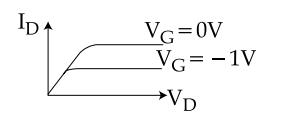
(c) n-channel FET (iii) 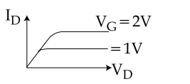
(d) p-channel Enhancement MOSFET (iv) 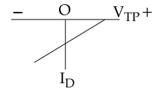
Codes :
The pull up to pull down ratio for an n mos inverter driven by another n mos inverter can be evaluated from:
(A) Vi nv = V t − \(\rm\frac{V_{t d}}{\sqrt{Zpu/Zpd}}\)
(B) V inv = \(\rm\frac{−V_{t d}}{\sqrt{Zpu/Zpd}}\)
(C) \(\rm\frac{W_{pd}}{L_{pd}}\) (V inv − V t) 2= \(\rm\frac{W_{p u}}{L_{p u}}\) (−V td )2
(D) \(\rm\frac{W_{p d}}{L_{p d}}\) (V inv − V t ) = \(\rm\frac{W_{p u}}{L_{pu}}\) (−V td )2
Choose the correct answer from the options given below:
Which of the following is NOT a minority carrier semiconductor device ?
The metal gate that is insulated from the channel is also referred to as: