
A MOSFET differs from the JFET because 1. of the characteristics 2. the MOSFET has two gates 3. the JFET has p-n junctions 4. of the physical reduced size
1 & 3
Statement 3 names the fundamental structural difference and statement 1 names its visible consequence — so the answer is 1 & 3, option 2.
Statement 3 — the physics. A JFET's gate is a reverse-biased p-n junction, and its depletion region squeezes the channel. A MOSFET's gate is a metal or polysilicon plate separated from the channel by an insulating oxide; there is no junction anywhere near it. That one difference produces every other:
| JFET | MOSFET | |
|---|---|---|
| Gate | p-n junction | Insulated by SiO2 |
| Gate current | Small leakage, nA | Essentially zero, pA |
| Input impedance | ~109 Ω | ~1014 Ω |
| Gate polarity | Reverse bias only | Either polarity |
| Modes | Depletion only | Depletion and enhancement |
Statement 1 — the characteristics. This follows directly. Because the JFET's gate junction must stay reverse biased, forward bias would make it conduct, so the gate can only ever reduce the channel: the JFET is a depletion-mode device with the channel present at \(V_{GS}=0\). The MOSFET's oxide permits gate voltage of either sign, so an enhancement device is possible, one with no channel at all until the gate creates an inversion layer:
\(I_{D}=K\left(V_{GS}-V_{T}\right)^{2}\qquad\text{for}\ V_{GS}\gt V_{T}\)
Its transfer curve sits entirely in the positive \(V_{GS}\) region, while the JFET's lies entirely in the negative — visibly different characteristics.
Why statement 2 is false. A MOSFET has one gate. Dual-gate MOSFETs exist and are used as mixers and AGC amplifiers, but they are a special type, not what distinguishes MOSFETs from JFETs. The four-terminal MOSFET's extra terminal is the substrate or body, not a second gate.
Why statement 4 is false as a distinguishing reason. MOSFETs are indeed the smaller devices — which is why integrated circuits are built from them and not from JFETs — but small size is a consequence of the fabrication process, not the reason the two device types differ in operation. The question asks what makes a MOSFET a different device.
Hence, statements 1 and 3 are correct.
Similar Questions
Match the following :
List - I List - II (figure in the original question) (a) n-channel Enhancement (Normally off) (i) 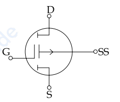
(b) p-channel Depletion MOSFET (Normally on) (ii) 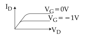
(c) n-channel FET (iii) 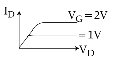
(d) p-channel Enhancement MOSFET (iv) 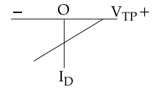
Codes :
Important Questions from Types of FET
The transconductance g mof a JFET is equal to:
\(\frac{ I _{ DSS }}{ V _{ P }}\left(1-\frac{ V _{ GS }}{ V _{ P }}\right)\)
The CMOS inverter can be used as an amplifier when:
In JFET, the Pinch‐off Voltage can be defined as:
In JFET, the current density in the x-direction is:
A. σ(x)E x
B. qN DμE x
C. \(\rm \frac{q}{2 \in_s}N_D\mu\)
D. \(\rm \frac{N_D\mu}{2 \in_s}\)
Choose the correct answer from the options given below:
Match List I with List II
List – I
List – II
JFET - Bias
Characteristic Equation
A.
Self - bias
I.
\(\rm I_D = \frac{V_{SS}-V_{GS}}{R_S}\)
B.
Voltage – divider bias
II.
\(\rm I_D = \frac{V_{EE}-V_{BE}}{R_E}\)
C.
Source bias
III.
V GS = -I DR S
D.
Current – source bias
IV.
\(\rm I_D = \frac{V_{G}-V_{GS}}{R_S}\)
Choose the correct answer from the options given below:



