
For the n-channel MOSFET shown in the figure given below, threshold voltage Vth = 2 V. The drain current ID of the MOSFET is 4 mA when the drain resistance RD is 1 kΩ. If the value of RD is increased to 4 kΩ, then the drain current ID will become :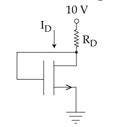
2.8 mA
The official answer key records option 1, 2.8 mA. That figure cannot be produced by the circuit as printed, so the working is set out in full below and the discrepancy is stated plainly rather than papered over.
The circuit. The gate is tied back to the drain, so this is a diode-connected n-channel MOSFET with its source grounded. Two consequences follow immediately :
| Consequence | Why |
|---|---|
| \(V_{GS}=V_{DS}\) | Gate and drain are the same node |
| The device is always in saturation | Saturation needs \(V_{DS}\ge V_{GS}-V_{th}\); here \(V_{DS}=V_{GS}\), which exceeds \(V_{GS}-V_{th}\) for any positive \(V_{th}\) |
So the square-law applies throughout: \(I_{D}=k\left(V_{GS}-V_{th}\right)^{2}\).
Step 1 — extract k from the given operating point. With \(R_{D}=1\,\text{k}\Omega\) and \(I_{D}=4\,\text{mA}\),
\(V_{DS}=10-\left(4\,\text{mA}\right)\left(1\,\text{k}\Omega\right)=6\ \text{V}=V_{GS}\)
\(4=k\left(6-2\right)^{2}=16k\quad\Rightarrow\quad k=0.25\ \text{mA/V}^{2}\)
Step 2 — solve the load line with \(R_{D}=4\,\text{k}\Omega\). Writing \(V\) for the new \(V_{DS}=V_{GS}\), the device equation and the load line must hold together :
\(I_{D}=0.25\left(V-2\right)^{2}\qquad\text{and}\qquad I_{D}=\dfrac{10-V}{4}\)
\(0.25\left(V-2\right)^{2}=\dfrac{10-V}{4}\ \Rightarrow\ \left(V-2\right)^{2}=10-V\ \Rightarrow\ V^{2}-3V-6=0\)
\(V=\dfrac{3+\sqrt{33}}{2}\approx 4.37\ \text{V}\qquad\Rightarrow\qquad I_{D}=\dfrac{10-4.37}{4}\approx \mathbf{1.4\ mA}\)
Step 3 — the sanity check that settles the matter. Whatever the transistor does, the drain current has to flow through \(R_{D}\) from a 10 V rail. The absolute ceiling is reached only if the transistor were a short circuit:
\(I_{D(\max)}=\dfrac{10\ \text{V}}{4\ \text{k}\Omega}=2.5\ \text{mA}\)
2.8 mA exceeds that ceiling, and would require \(V_{DS}=10-2.8\times 4=-1.2\ \text{V}\) — a negative drain voltage from a positive supply. It is not a close call or a rounding question; the keyed value is unreachable.
The physical reasoning also points downward. Raising \(R_{D}\) from 1 kΩ to 4 kΩ drops more voltage across the resistor, which pulls the drain — and therefore the gate — lower, which reduces \(V_{GS}-V_{th}\) and so reduces the current. In a diode-connected device the current must fall when the load resistance rises. Option 1 is the only choice larger than the original 4 mA would allow after that fall, while 1.4 mA sits exactly where the algebra puts it.
Note on the recorded answer. The answer stored here follows the official key, as required. On the physics the defensible answer is option 3, 1.4 mA.
Similar Questions
The threshold voltage of an n-channel MOSFET can be increased by
Assertion (A) : MOS ICs based on MOSFET structure find wide applications in digital field.
Reason (R) : MOS ICs have small size and are easy to fabricate.
In MOSFET, the carrier velocity between constant mobility regime and the saturation velocity can be described as :
If Z × L is the total channel area and C'par is the total input parasitic capacitance, then for microwave performance the cut off frequency can be defined as :
(A) \(\dfrac{g_{m}}{2\pi\left(C'_{ca}+C'_{par}\right)}\)
(B) \(\dfrac{g_{m}}{2\pi C_{gs}}\)
(C) \(\dfrac{g_{m}}{2\pi C_{gd}}\)
(D) \(\dfrac{g_{m}}{2\pi\left(ZLC_{ox}+C'_{par}\right)}\)Choose the most appropriate answer from the options given below :
Consider the following statements :
(A) The origin of the punch through phenomena is the lowering of the barrier near the source.
(B) For a long channel device, a drain bias can change the effective channel length, but the barrier at the source end remains constant.
(C) For a short channel device, this barrier is no longer fixed.
(D) The lowering of the source barrier do not cause any injection of extra carriers.
(E) The punch through condition normally occurs inside the bulk region of the semiconductor.Choose the most appropriate answer from the options given below :
In MOSFET, the linear region current is :
(A) \(\dfrac{\mu_{n}C_{ox}w}{L}\left(V_{gs}-V_{th}-\dfrac{V_{ds}}{2}\right)V_{ds}\)
(B) \(\dfrac{\mu_{n}C_{ox}w}{L}\left(V_{gs}-V_{th}\right)V_{ds}\)
(C) \(\dfrac{\mu_{n}C_{ox}w}{2L}\left(V_{gs}-V_{th}\right)V_{ds}^{2}\)
(D) \(\dfrac{\mu_{n}C_{ox}w}{L}\left(V_{gs}-V_{th}\right)^{2}\)Choose the most appropriate answer from the options given below :
Approximate oxide capacitance value (Cgd) for saturation operating mode of MOS transistor is:
For an n-channel MOS transistor with $\mu_n$ = 600 cm2/Vs, Cox = 7 x 10⁻⁸ F/cm2, W = 40 $\mu_m$, L = 4$\mu_m$ and VTO=1.0 V, the value of K parameter is:
In MOS
A. The substrate fermi potential ϕF is negative in NMOS
B. The substrate fermi potential ϕF is positive in NMOS
C. The substrate bias voltage VSB is positive in NMOS, negative in PMOS
D. The substrate bias voltage VSB is negative in NMOS, positive in PMOS.
Choose the correct answer from the options given below:
In enhancement mode MOSFET the saturation (drain) current is given by
(a) \(K\dfrac{W}{L}(V_{gs}-V_{th})^{2}\)
(b) \(K\dfrac{W}{L}(V_{gs}-V_{th})(1+\lambda V_{ds})\)
(c) \(K\dfrac{W}{L}(V_{gs}-V_{th})^{2}(1+\lambda V_{ds})\)
(d) \(K\dfrac{W}{L}(V_{gs}-V_{th})^{2}(1-\lambda V_{ds})\)
Out of these
Important Questions from MOSFET
The O in a MOSFET stands for _______ layer which provides _______ to the device.
Which industry does aluminium smelting belong to?
In an N-channel MOSFET, the drain current ID increases as _______.
Consider an ideal long channel nMOSFET (enhancement-mode) with gate length 10 µm and width 100 µm. The product of electron mobility (µn) and oxide capacitance per unit area (COX) is µn COX = 1 mA/V2 . The threshold voltage of the transistor is 1 V. For a gate-to-source voltage VGS = [2 − sin (2t)] V and drain-to-source voltage VDS = 1 V (substrate connected to the source), the maximum value of the drain-to-source current is ________.
- A power MOSFET is a ___________, __________ controlled and ___________ carrier device.



