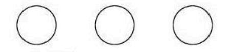
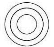
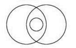
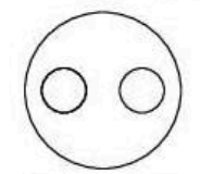
A. Passivation
B. n-well implant
C. Metallization
D. Source/drain diffusion
Choose the correct answer from the options given below :
The process of n-well fabrication in integrated circuit manufacturing is a critical part of the CMOS technology. It requires a precise sequence of steps to ensure the proper formation of the well and the subsequent components. Here's a detailed breakdown of the correct sequence:
- n-well implant (B): At this stage, the n-well is created by implanting donor atoms like phosphorus or arsenic into the silicon substrate. This forms the n-type region necessary for the CMOS transistor.
- Source/drain diffusion (D): After the n-well is formed, the source and drain regions of the transistors are defined and dopants are diffused into these regions to form the source-drain junctions of the transistor.
- Metallization (C): This step involves depositing metal contacts to connect the various parts of the circuit. The most commonly used metal is aluminum, which is deposited using techniques like sputtering or chemical vapor deposition.
- Passivation (A): The final step involves depositing a passivation layer, typically silicon dioxide or silicon nitride, to protect the wafer's surface and the integrated circuit from external contaminants and physical damage.
Therefore, the correct sequence for the n-well fabrication process is B, D, C, A. This ensures that each component is correctly aligned and functional for the integrated circuit's overall performance.
Thus, the correct answer is: B, D, C, A
Similar Questions
- Calculate the output voltage of an op-amp for input voltages of $V_{i1} = 150 \mu\text{V}$ and $V_{i2} = 140 \mu\text{V}$. The amplifier has a differential gain of $A_d = 4000$ and the value of CMRR is $100$ :
- For an op-amp having a slew rate of $4\text{ V}/\mu\text{s}$, what is the maximum closed-loop voltage gain that can be used when input signal varies by $0.1\text{V}$ in $10\mu\text{s}$ ?
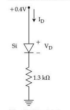
For the series diode configuration of the given figure, determine $V_D$ and $I_D$.
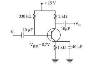
For the given emitter-bias network, determine the values of $I_C$ and $V_{CE}$. Assume $\beta = 100$.
- Given below are two statements : one is labelled as Assertion (A) and the other is labelled as Reason (R).
Assertion (A) : The gate of a MOSFET is insulated from body of FET by deposition of a very thin fragile layer of $\text{SiO}_2$ over the substrate.
Reason (R) : The device is therefore called an insulated gate field-effect transistor (IGFET).
In the light of the above statements, choose the most appropriate answer from the options given below : - Given below are two statements : one is labelled as Assertion (A) and the other is labelled as Reason (R).
Assertion (A) : The body effect in MOSFET causes the threshold voltage $V_{\text{th}}$ to increase as source-body voltage $V_{\text{SB}}$ increases.
Reason (R) : Increasing $V_{\text{SB}}$ raises the surface potential and therefore reduces the barrier for inversion.
In the light of the above statements, choose the most appropriate answer from the options given below : - What is the typical efficiency of half-wave rectifier:
- The sequence of physical events when forward bias is applied to PN junction:
A. Barrier potential reduces
B. Majority carriers injected across junction
C. Recombination in neutral regions increases
D. Diffusion current established across quasi-neutral regions
E. Net forward current increases
Choose the correct answer from the options given below : - In an op-amp which of the following parameters depend on frequency.
A. Voltage gain
B. Noise current
C. CMRR
D. Output voltage swing
E. Gain bandwidth product
Choose the correct answer from the options given below : - Which of the following statements are correct:
A. A negative feedback can increase linearity and reduce distortion.
B. Positive feedback always improves stability of the amplifier.
C. Series-shunt (Voltage) negative feedback tends to reduce output impedance.
D. Closed-loop bandwidth typically increased when negative feedback is applied.
Choose the correct answer from the options given below :
Important Questions from Miscellaneous
- Which of the following relationships is/are not true?
(A). Most probable velocity = $\sqrt{\frac{2RT}{M}}$
(B). PV = $\frac{3}{2}kT$
(C). Compressibility factor Z = $\frac{pV}{nRT}$
(D). Average kinetic energy of gas = $\frac{1}{2}kT$
Choose the correct answer from the options given below - Match List-I with List-II
List-I List-II Electronic Configuration First Ionisation energy (kJ mol$^{-1}$) (A). ns$^2$ (I). 2100 (B). ns$^2$np$^1$ (II). 1400 (C). ns$^2$np$^3$ (III). 800 (D). ns$^2$np$^6$ (IV). 900
Choose the correct answer from the options given below: - The shielding constant of a 2p electron (calculated using Slater's rules) is
- Match List-I with List-II
List-I List-II Spectroscopy Property (A). Raman (I). Polarizability (B). FTIR (II). Dipole Moment (C). UV-Visible (III). Absorbance (D). NMR (IV). Spin
Choose the correct answer from the options given below: - The structure of protein comprises of:
(A). Primary structure of protein is associated with amino acids
(B). Secondary structure of protein is associated to peptides
(C). Tertiary structure of protein is associated with polypeptide chains
(D). Quaternary structure of protein is associated with polypeptide chains
Choose the correct answer from the options given below: