
Match the following : Codes :List – I List – II a. 7400 i. Quad-2 input AND gate b. 7402 ii. Quad-2 input OR gate c. 7408 iii. Quad-2 input NAND gate d. 7403 iv. Quad-2 input NOR gate
a-iii, b-iv, c-i, d-ii
Three of the four part numbers are among the most familiar in the 74 series, and they settle the answer between them :
| Part | Function | Match |
|---|---|---|
| 7400 | Quad 2-input NAND | iii |
| 7402 | Quad 2-input NOR | iv |
| 7408 | Quad 2-input AND | i |
| 7403 | Quad 2-input NAND, open collector | ii by elimination |
So the code is a-iii, b-iv, c-i, d-ii — option 2.
The 7400 is the anchor, and worth knowing for its own sake: it is the first device of the family and the reason NAND is called the universal gate. Every other function can be built from NANDs alone — an inverter by tying the inputs together, an AND by inverting a NAND's output, an OR by inverting both inputs of a NAND — which is why the 7400 became the most-produced logic part ever made.
A defect in the question, worth stating plainly. There is no quad 2-input OR gate numbered 7403; the real 7403 is a quad NAND with open-collector outputs, and the quad OR gate in the family is the 7432. Since List II offers each function once and 7400, 7402 and 7408 are unambiguous, the remaining item can only pair with the remaining function, and option 2 is the intended answer. The mismatch is in the paper, not in the reasoning.
What "open collector" means explains why 7403 exists alongside 7400 at all. Its output transistor can pull down but not up, so an external pull-up resistor is needed. The advantage is that several such outputs may be tied together on one line: any one of them can pull it low, giving a wired-AND without extra gates, and allowing the line to be driven to a different voltage from the logic supply — which is how open-collector parts drive relays, LEDs and shared buses.
The numbering has no logic to it beyond history; the parts were numbered as they were introduced. The three to hold in memory are 7400 NAND, 7402 NOR, 7404 hex inverter, with 7408 AND and 7432 OR close behind.
Hence, the correct code is a-iii, b-iv, c-i, d-ii.
Similar Questions
If the output of a logic gate is zero when all its inputs are at logic 1. The gate is either
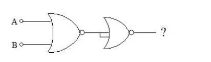
Compute output of following logic gates as combinational circuit.
Match the following lists in terms of qualifying symbols for inputs and outputs :
List - I List - II a. 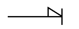
i. Non-logic connection b. 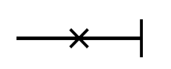
ii. Input for digital signals c. 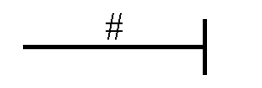
iii. Logic negation at the input d. 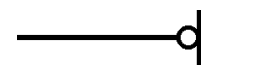
iv. Active low input Correct codes are :
Important Questions from Logic Gates
Which logical gate is included in a binary adder circuit to enable binary addition and subtraction?
A Circuit that operates in such a way that its output is high only when all its inputs are high
______ is also known as Inverter.
The minimum number of NAND gates required to reduce the expression ((A + B)C) D is:
In which of the following gates, the output is high if and only if all inputs are high?



