
Which one of the below referred figure represents the cut-off of npn or pnp transistor ?
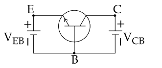
The rule that defines each region. A bipolar transistor's operating region is decided entirely by the bias on its two junctions:
| Region | Emitter junction | Collector junction |
|---|---|---|
| Active | forward | reverse |
| Saturation | forward | forward |
| Cut-off | reverse | reverse |
| Reverse active | reverse | forward |
So the answer is whichever figure reverse-biases both junctions.
Step 1 — read the transistor type from the emitter arrow. The arrow sits on the emitter lead and points away from the base for an npn and toward the base for a pnp. Options 1 and 2 are npn; option 3 is pnp.
Step 2 — translate the battery polarity for an npn. For npn the emitter junction is forward biased when the base is positive with respect to the emitter. A battery marked + on the emitter side makes \(V_{EB} \gt 0\), so \(V_{BE} \lt 0\) and the junction is reverse biased. Likewise \(V_{CB} \gt 0\) reverse biases the collector junction of an npn.
Option 1: VEB is negative at the emitter, so VBE is positive — emitter junction forward, collector junction reverse. That is the active region, not cut-off.
Option 2: both batteries positive at the outer terminal, so both junctions of the npn are reverse biased. This is cut-off ✓
Step 3 — why the pnp of option 3 fails. Every polarity requirement inverts for a pnp: its emitter junction is forward biased when the emitter is positive with respect to the base. With both batteries positive at the outer terminals, both of the pnp's junctions are forward biased — that is saturation, the opposite of what is wanted. Option 4 marks no polarity at all and so specifies nothing.
What cut-off means in the device. With both junctions reverse biased no carriers are injected, and only the tiny leakage ICEO flows — the transistor behaves as an open switch, with the collector sitting at the supply rail. Cut-off and saturation are the two states used in switching; the active region is reserved for amplification.
Hence, the npn with both VEB and VCB positive at the outer terminal represents cut-off.
Similar Questions
In a bipolar junction transistor, the collector current is
In a BJT the collector current in common emitter configuration is
Important Questions from Bipolar Junction Transistors
For a common emitter connection of BJT, find the value of β if α = 0.995
- Which represents the Transport Factor of BJT?
For a bipolar junction transistor in common emitter mode, IC = maximum and VC (collector voltage) = VE (emitter voltage), the transistor operates in _____ mode.
High frequency transistors are designed especially for:
- For an ideal transistor, the reverse parameters (h o& h r) are



