
During the p-n junction formation, when an electron diffuses from n → p, it leaves behind an:
Ionised donor on n-side
Understanding p-n Junction Formation and Electron Diffusion
A p-n junction is formed when a p-type semiconductor is joined with an n-type semiconductor. Both p-type and n-type semiconductors are formed by doping intrinsic semiconductors like silicon or germanium with impurities.
Composition of p-type and n-type Semiconductors
- n-type semiconductor: Created by doping with pentavalent impurities (like Phosphorus, Arsenic, Antimony). These impurities are called donor impurities because they donate an extra electron for conduction. When a donor atom gives up its electron, it becomes a positively charged ion ($D^+$) which is fixed in the crystal lattice. The majority carriers are electrons, and minority carriers are holes.
- p-type semiconductor: Created by doping with trivalent impurities (like Boron, Aluminum, Gallium). These impurities are called acceptor impurities because they accept an electron, creating a hole. When an acceptor atom accepts an electron, it becomes a negatively charged ion ($A^-$) which is fixed in the crystal lattice. The majority carriers are holes, and minority carriers are electrons.
The Process of p-n Junction Formation: Diffusion
When the p-type and n-type materials are brought together to form a junction, there are high concentrations of electrons in the n-side and high concentrations of holes in the p-side. Due to this concentration difference, charge carriers begin to diffuse across the junction:
- Electrons diffuse from the n-side to the p-side.
- Holes diffuse from the p-side to the n-side.
What Happens During Electron Diffusion from n → p?
Let's focus on the diffusion of an electron from the n-side towards the p-side. In the n-type material, donor atoms have contributed free electrons. The donor atom itself is initially neutral. When one of its loosely bound electrons diffuses away from the n-side across the junction:
- The electron moves from the n-side into the p-side.
- On the n-side, the donor atom that was associated with this electron is left behind.
- Since the electron (negative charge) has left, the donor atom which was initially neutral now has a net positive charge. It becomes an ionised donor atom ($D^+$).
- These ionised donor atoms are fixed in the crystal lattice and cannot move across the junction.
- As electrons continue to diffuse from the n-side and leave behind these positive ions, a region near the junction on the n-side becomes populated with fixed positive charges.
Similarly, when holes diffuse from the p-side to the n-side, they leave behind fixed negative acceptor ions ($A^-$) on the p-side near the junction.
The region around the junction that is depleted of mobile charge carriers (electrons and holes) and contains only fixed positive and negative ions is called the depletion region or depletion layer.
Analyzing the Options
The question asks what is left behind on the n-side when an electron diffuses from n → p.
- Option 1: Ionised acceptor on n-side. Incorrect, acceptor ions are in the p-type material.
- Option 2: Ionised donor on n-side. Correct, when an electron leaves a donor atom on the n-side, the donor atom becomes a positive ion fixed in the lattice.
- Option 3: Ionised donor on p-side. Incorrect, donor atoms are in the n-type material.
- Option 4: Ionised donor on n-side and p-side both. Incorrect, the primary source of donor ions is the n-side.
Therefore, when an electron diffuses from n → p, it leaves behind an ionised donor on the n-side.
Revision Table: Key Concepts in p-n Junction Formation
| Concept | Description | Relevant to Electron Diffusion n → p |
|---|---|---|
| n-type Semiconductor | Doped with donors, excess electrons, fixed $D^+$ ions after ionization. | Source of diffusing electrons; location where $D^+$ ions are left behind. |
| p-type Semiconductor | Doped with acceptors, excess holes, fixed $A^-$ ions after accepting electron. | Destination of diffusing electrons. |
| Diffusion | Movement of carriers from high concentration to low concentration. | Driving force for initial electron flow from n → p. |
| Electron Diffusion (n → p) | Electrons move from n-side to p-side. | This specific process leaves behind positively charged entities on the n-side. |
| Ionised Donor ($D^+$) | A donor atom that has lost its extra electron, fixed positive charge. | This is exactly what is left behind on the n-side when an electron diffuses away. |
Additional Information: Depletion Region and Built-in Potential
The formation of the fixed positive ions ($D^+$) on the n-side and fixed negative ions ($A^-$) on the p-side near the junction creates a region devoid of mobile charge carriers. This region is called the depletion region.
The fixed charges in the depletion region create an electric field directed from the positive ions on the n-side to the negative ions on the p-side. This electric field opposes further diffusion of carriers across the junction.
This electric field corresponds to a potential difference across the junction, known as the built-in potential or barrier potential ($V_0$). The barrier potential prevents most of the majority carriers from crossing the junction under equilibrium conditions.
The balance between the diffusion current (due to concentration gradient) and the drift current (due to the built-in electric field) establishes equilibrium in the p-n junction with no external bias.
Important Questions from Semiconductor and Electronic Devices
If the forward voltage in a p-n junction diode is increased, the width of the depletion region:
Two identical thin metal plates are given charges q1 and q2 (q2 < q1) respectively. If they are now brought close together to form a parallel plate capacitor with a capacitance 'C', then the potential difference between the plates is:
Displacement current (id) = ω0 dΦE / dt. Where symbols have their usual meanings. Which of the following options gives correct equation for displacement current?
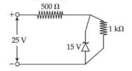
A Zener diode is used in a voltage regulator circuit as shown below. Its breakdown voltage is 15 V. What is the current flowing through the Zener diode?
Choose the correct experimental circuit arrangement for studying V-I characteristics of a p-n junction diode in forward bias:


