
If the forward voltage in a p-n junction diode is increased, the width of the depletion region:
Decreases
In a p-n junction diode, the depletion region is formed due to the diffusion of charge carriers, creating an electric field.
- In forward bias, applying a positive voltage reduces the built-in potential, allowing more charge carriers to flow.
- As a result, the depletion width decreases because the external voltage reduces the barrier for charge movement.
Thus, the correct answer is (b).
Important Questions from Semiconductor and Electronic Devices
Silicon can be doped using one of the following elements as dopant:
(A) Arsenic
(B) Indium
(C) Phosphorus
(D) BoronTo get an n-type semiconductor, the dopants that can be used are:
Let iE, iC, and iB represent the emitter current, collector current, and the base current respectively in a transistor. Choose the correct statement:
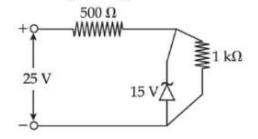
A Zener diode is used in a voltage regulator circuit as shown below. Its breakdown voltage is 15 V. What is the current flowing through the Zener diode?
Choose the correct experimental circuit arrangement for studying V-I characteristics of a p-n junction diode in forward bias:
During the p-n junction formation, when an electron diffuses from n → p, it leaves behind an:


