
Silicon can be doped using one of the following elements as dopant: (A) Arsenic To get an n-type semiconductor, the dopants that can be used are:
(B) Indium
(C) Phosphorus
(D) Boron
(A) and (C) only
Let's break down how doping works in semiconductors like Silicon and which elements help create an n-type material. Silicon (Si) is a semiconductor from Group 14 of the periodic table, meaning it has 4 valence electrons. To change its electrical properties, we add impurities in a process called doping.
Understanding N-Type Semiconductor Doping
An n-type semiconductor is created when we dope a pure (intrinsic) semiconductor like Silicon with donor impurities. Donor impurities are elements that have more valence electrons than the semiconductor material. For Silicon (4 valence electrons), suitable donor impurities come from Group 15 of the periodic table, which have 5 valence electrons. When a Group 15 element replaces a Silicon atom in the crystal lattice, four of its valence electrons form covalent bonds with the surrounding Silicon atoms, just like a Silicon atom would. However, the fifth valence electron is left loosely bound and becomes a free electron, which can move easily and carry electric current. These free electrons are the majority charge carriers in an n-type semiconductor.
Analyzing the Potential Dopants for Silicon
The question provides four potential dopants for Silicon: Arsenic, Indium, Phosphorus, and Boron. Let's look at their positions in the periodic table and their number of valence electrons:
- (A) Arsenic (As): Arsenic is in Group 15. It has 5 valence electrons.
- (B) Indium (In): Indium is in Group 13. It has 3 valence electrons.
- (C) Phosphorus (P): Phosphorus is in Group 15. It has 5 valence electrons.
- (D) Boron (B): Boron is in Group 13. It has 3 valence electrons.
To create an n-type semiconductor from Silicon, we need donor impurities from Group 15 (pentavalent impurities). These are elements with 5 valence electrons. Looking at the list, both Arsenic (A) and Phosphorus (C) are in Group 15. They will donate an extra electron when substituted into the Silicon lattice, resulting in an n-type semiconductor.
Elements from Group 13 (trivalent impurities) like Indium (B) and Boron (D) have 3 valence electrons. When they replace a Silicon atom, they create a deficiency of one electron, forming a "hole". These holes are the majority charge carriers in a p-type semiconductor.
Therefore, to obtain an n-type semiconductor by doping Silicon, we can use Arsenic (A) or Phosphorus (C).
Let's summarize the effect of each dopant:
| Dopant | Element Symbol | Group | Valence Electrons | Type of Impurity | Semiconductor Type Created (with Silicon) |
|---|---|---|---|---|---|
| Arsenic | As | 15 | 5 | Donor (Pentavalent) | n-type |
| Indium | In | 13 | 3 | Acceptor (Trivalent) | p-type |
| Phosphorus | P | 15 | 5 | Donor (Pentavalent) | n-type |
| Boron | B | 13 | 3 | Acceptor (Trivalent) | p-type |
Based on this analysis, the dopants that can be used to get an n-type semiconductor are Arsenic (A) and Phosphorus (C).
Conclusion on Silicon N-Type Dopants
The question asks for the dopants from the given list that can be used to get an n-type semiconductor. These are the Group 15 elements, Arsenic (A) and Phosphorus (C).
Revision Table: Key Semiconductor Doping Concepts
| Concept | Description | Example Dopants (for Si) | Majority Carriers |
|---|---|---|---|
| Intrinsic Semiconductor | Pure semiconductor material (e.g., Si, Ge) | None | Equal electrons and holes (very few) |
| Extrinsic Semiconductor | Doped semiconductor material | Donor (Group 15) or Acceptor (Group 13) | Electrons (n-type) or Holes (p-type) |
| n-type Semiconductor | Doped with donor impurities (more valence electrons) | P, As, Sb (Group 15) | Electrons |
| p-type Semiconductor | Doped with acceptor impurities (fewer valence electrons) | B, Al, Ga, In (Group 13) | Holes |
Additional Information on Doping Semiconductors
Doping is a crucial process in manufacturing semiconductor devices like diodes, transistors, and integrated circuits. The concentration of dopant atoms added determines the conductivity of the extrinsic semiconductor. A higher doping concentration leads to higher conductivity. Doping levels are typically measured in atoms per cubic centimeter, ranging from lightly doped (e.g., \(10^{14}\) atoms/cm\(^3\)) to heavily doped (e.g., \(10^{20}\) atoms/cm\(^3\)). The process is carefully controlled to achieve specific electrical characteristics required for different electronic components. Common methods for doping include diffusion and ion implantation.
Important Questions from Semiconductor and Electronic Devices
Let iE, iC, and iB represent the emitter current, collector current, and the base current respectively in a transistor. Choose the correct statement:
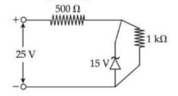
A Zener diode is used in a voltage regulator circuit as shown below. Its breakdown voltage is 15 V. What is the current flowing through the Zener diode?
Choose the correct experimental circuit arrangement for studying V-I characteristics of a p-n junction diode in forward bias:
During the p-n junction formation, when an electron diffuses from n → p, it leaves behind an:
A Zener diode is used in a voltage regulator circuit as shown below. Its breakdown voltage is 15 V. What is the current flowing through the Zener diode?


