
Let iE, iC, and iB represent the emitter current, collector current, and the base current respectively in a transistor. Choose the correct statement:
iE is equal to the sum of iC and iB
Understanding the relationship between the currents in a transistor is fundamental to semiconductor electronics. A bipolar junction transistor (BJT) has three terminals: the emitter, the base, and the collector. Current flows into or out of each of these terminals.
Transistor Current Relationships
In a transistor, the total current entering or leaving the device must balance. According to Kirchhoff's Current Law (KCL) applied to the transistor, the current entering the emitter terminal (\(i_E\)) is the sum of the current leaving the base terminal (\(i_B\)) and the current leaving the collector terminal (\(i_C\)). This forms a basic equation relating the three currents:
\(i_E = i_C + i_B\)
This equation holds true for both NPN and PNP transistors, though the direction of current flow is reversed between the two types.
Analyzing the Options for Transistor Currents
Let's examine each given statement based on the fundamental transistor current equation \(i_E = i_C + i_B\):
- Option 1: \(i_C\) is slightly greater than \(i_E\)
This statement is incorrect. The emitter current (\(i_E\)) is the sum of the collector current (\(i_C\)) and the base current (\(i_B\)). Since the base current (\(i_B\)) is typically a small but non-zero value, the collector current (\(i_C\)) will always be slightly less than the emitter current (\(i_E\)), not greater. \(i_C \approx i_E\), but \(i_C < i_E\). - Option 2: \(i_B\) is much greater than \(i_E\)
This statement is incorrect. The base current (\(i_B\)) is a very small fraction of the total emitter current (\(i_E\)). The emitter current is the sum of the base and collector currents (\(i_E = i_C + i_B\)), and \(i_C\) constitutes the majority of \(i_E\). Therefore, \(i_B\) is much less than \(i_E\), not greater. - Option 3: \(i_C\) is equal to \(i_B\)
This statement is incorrect. The collector current (\(i_C\)) is typically much larger than the base current (\(i_B\)). The ratio of collector current to base current is the current gain (\(\beta\)) of the transistor, where \(i_C = \beta i_B\). Since \(\beta\) is usually much greater than 1 (typically 50 to 300 or more), \(i_C\) is much greater than \(i_B\). - Option 4: \(i_E\) is equal to the sum of \(i_C\) and \(i_B\)
This statement is correct. As established by Kirchhoff's Current Law for the transistor, the emitter current (\(i_E\)) is indeed the sum of the collector current (\(i_C\)) and the base current (\(i_B\)). This is the fundamental relationship governing the currents in a bipolar junction transistor.
Therefore, the correct statement describing the relationship between the emitter current (\(i_E\)), collector current (\(i_C\)), and base current (\(i_B\)) in a transistor is that \(i_E\) is equal to the sum of \(i_C\) and \(i_B\).
Revision Table: Transistor Current Relationships
| Current | Symbol | Typical Magnitude Relation | Role |
|---|---|---|---|
| Emitter Current | \(i_E\) | Largest current; \(i_E = i_C + i_B\) | Total input/output current; Carries both majority & minority carriers |
| Collector Current | \(i_C\) | Majority of \(i_E\); \(i_C \approx i_E\) | Output current; Controlled by \(i_B\) |
| Base Current | \(i_B\) | Smallest current; \(i_B = i_E - i_C\) | Input current that controls \(i_C\) |
Additional Information on Transistor Currents
The current relationship \(i_E = i_C + i_B\) is a direct application of charge conservation within the transistor. Emitter current consists of carriers (electrons in NPN, holes in PNP) injected into the base region. Most of these carriers diffuse across the thin base and are collected by the collector. A small fraction of the carriers combine with the majority carriers in the base, forming the base current.
The performance of a transistor is often described by two current gain parameters:
- Beta (\(\beta\)) or hFE: This is the common-emitter current gain, defined as the ratio of collector current to base current: \(\beta = \frac{i_C}{i_B}\). This parameter indicates how much the base current controls the collector current.
- Alpha (\(\alpha\)) or hFB: This is the common-base current gain, defined as the ratio of collector current to emitter current: \(\alpha = \frac{i_C}{i_E}\). Alpha is typically close to 1, usually between 0.95 and 0.99.
These parameters are related by the equations:
\(\beta = \frac{\alpha}{1 - \alpha}\)
\(\alpha = \frac{\beta}{1 + \beta}\)
Knowing \(i_E = i_C + i_B\) is the fundamental starting point for analyzing transistor circuits.
Important Questions from Semiconductor and Electronic Devices
Silicon can be doped using one of the following elements as dopant:
(A) Arsenic
(B) Indium
(C) Phosphorus
(D) BoronTo get an n-type semiconductor, the dopants that can be used are:
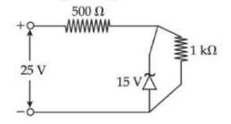
A Zener diode is used in a voltage regulator circuit as shown below. Its breakdown voltage is 15 V. What is the current flowing through the Zener diode?
Choose the correct experimental circuit arrangement for studying V-I characteristics of a p-n junction diode in forward bias:
During the p-n junction formation, when an electron diffuses from n → p, it leaves behind an:
A Zener diode is used in a voltage regulator circuit as shown below. Its breakdown voltage is 15 V. What is the current flowing through the Zener diode?


