
Which of the following causes electric conduction in a semiconductor?
Both electrons and holes
Understanding Electric Conduction in Semiconductors
Electric conduction, or the flow of electric current, in any material depends on the availability and movement of charge carriers. In different materials, the primary charge carriers can vary. For example, in metals (conductors), electric conduction is primarily due to the movement of free electrons. In electrolytes, it's due to the movement of ions. Semiconductors are a class of materials that exhibit conductivity between that of conductors and insulators. The mechanism of electric conduction in semiconductors is unique because it involves two types of charge carriers.
Role of Electrons in Semiconductor Conduction
In a semiconductor material, electrons in the valence band are normally bound to atoms. However, with sufficient energy (like thermal energy or energy from light), some electrons can break free from their covalent bonds and move into the conduction band. Once in the conduction band, these electrons are free to move throughout the crystal lattice and contribute to electric conduction. These free electrons carry a negative charge and move towards the positive terminal of an applied electric field.
Role of Holes in Semiconductor Conduction
When an electron moves from the valence band to the conduction band, it leaves behind a vacancy in the valence band. This vacancy is called a "hole". While a hole is not a physical particle, it behaves like a positive charge because the absence of a negatively charged electron effectively creates a positive charge relative to the surrounding neutral atoms. When an electric field is applied, an electron from a neighboring bond can move into this hole, filling it. This leaves a new hole in the position previously occupied by that electron. This process continues, and the hole appears to move through the valence band in the direction of the electric field, opposite to the movement of electrons. The movement of holes also constitutes an electric current.
Combined Conduction by Electrons and Holes
Therefore, in semiconductors, electric conduction occurs through the movement of both free electrons in the conduction band and holes in the valence band. The total current is the sum of the electron current and the hole current.
Based on this understanding, let's analyze the given options for electric conduction in a semiconductor:
- Holes only: This is incorrect because electrons also contribute to conduction in semiconductors.
- Electrons only: This is incorrect because holes also contribute to conduction in semiconductors. While electrons are the sole carriers in metals, semiconductors are different.
- Both electrons and holes: This is correct. Electric conduction in semiconductors is due to the movement of both free electrons and holes.
- Neither holes nor electrons: This is incorrect. Semiconductors do conduct electricity, and this conduction is facilitated by charge carriers (electrons and holes).
Thus, the electric conduction in a semiconductor is caused by both electrons and holes.
| Material Type | Primary Charge Carriers |
|---|---|
| Conductor (e.g., Metals) | Free Electrons |
| Semiconductor (e.g., Silicon, Germanium) | Electrons and Holes |
| Insulator (e.g., Rubber, Glass) | Very Few Charge Carriers |
| Electrolyte Solutions | Positive and Negative Ions |
Revision Table: Semiconductor Conduction
| Concept | Description | Charge | Contribution to Conduction |
|---|---|---|---|
| Electron | Electron in the conduction band, free to move. | Negative ($-e$) | Yes, movement is current. |
| Hole | Vacancy left by an electron in the valence band. | Positive ($+e$) | Yes, movement of the vacancy is current. |
| Valence Band | Energy band where valence electrons are normally located. | N/A | Hole movement occurs here. |
| Conduction Band | Higher energy band where free electrons reside. | N/A | Electron movement occurs here. |
Additional Information on Semiconductor Charge Carriers
Semiconductors can be broadly classified into intrinsic and extrinsic semiconductors.
- Intrinsic Semiconductors: These are pure semiconductors (like pure silicon or germanium). In intrinsic semiconductors, electrons and holes are generated in pairs (when an electron breaks a bond and moves to the conduction band, a hole is left behind). Thus, the number of free electrons ($n$) is equal to the number of holes ($p$). Conduction is equally contributed by both.
- Extrinsic Semiconductors: These are semiconductors doped with impurities to increase their conductivity.
- n-type semiconductors: Doped with donor impurities (like Phosphorus in Silicon) which donate extra electrons. In these, electrons are the majority carriers, and holes are the minority carriers. Conduction is primarily by electrons, but holes still contribute.
- p-type semiconductors: Doped with acceptor impurities (like Boron in Silicon) which create extra holes. In these, holes are the majority carriers, and electrons are the minority carriers. Conduction is primarily by holes, but electrons still contribute.
In all types of semiconductors (intrinsic, n-type, or p-type), electric conduction involves the movement of both electrons and holes, although their relative contributions might differ in extrinsic types.
Important Questions from Semiconductor and Electronic Devices
Silicon can be doped using one of the following elements as dopant:
(A) Arsenic
(B) Indium
(C) Phosphorus
(D) BoronTo get an n-type semiconductor, the dopants that can be used are:
Let iE, iC, and iB represent the emitter current, collector current, and the base current respectively in a transistor. Choose the correct statement:
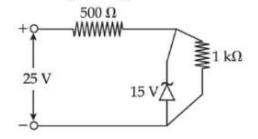
A Zener diode is used in a voltage regulator circuit as shown below. Its breakdown voltage is 15 V. What is the current flowing through the Zener diode?
Choose the correct experimental circuit arrangement for studying V-I characteristics of a p-n junction diode in forward bias:
During the p-n junction formation, when an electron diffuses from n → p, it leaves behind an:


