Which of the following gates can give an AND gate by its repetitive use?
Both NAND gate and NOR gate
Understanding Universal Logic Gates
In digital electronics, some logic gates are considered 'universal'. This means that any other logic gate (like AND, OR, NOT, XOR, XNOR) can be implemented using only this single type of gate, repeated as many times as needed. The two most common universal gates are the NAND gate and the NOR gate.
The question asks which gate(s) can produce an AND gate through repetitive use. Let's examine the possibilities for NAND and NOR gates.
Constructing an AND Gate Using Only NAND Gates
A NAND gate produces the inverse of an AND gate's output. The output of a NAND gate with inputs A and B is \( \overline{A \cdot B} \). To get the AND output \( A \cdot B \), we need to invert the NAND output.
A NOT gate can be formed by connecting both inputs of a NAND gate together. If the input is A, the output of a NAND gate with both inputs connected to A is \( \overline{A \cdot A} = \overline{A} \).
So, to build an AND gate from a NAND gate, we can:
- First, use a NAND gate with inputs A and B. This gives \( \overline{A \cdot B} \).
- Then, feed the output \( \overline{A \cdot B} \) into another NAND gate configured as a NOT gate (by connecting its inputs together).
The final output will be \( \overline{(\overline{A \cdot B})} = A \cdot B \), which is the AND function.
Let's look at the logic and truth table:
Logic: AND(A, B) = NOT(NAND(A, B))
Circuit representation using only NAND gates:
A --[NAND]--+--[NAND]-- Output \( A \cdot B \)
B --[NAND]--+
Where the second NAND gate has its inputs tied together.
| A | B | NAND(A, B) (\( \overline{A \cdot B} \)) | NOT(NAND(A, B)) (\( \overline{\overline{A \cdot B}} = A \cdot B \)) |
|---|---|---|---|
| 0 | 0 | 1 | 0 |
| 0 | 1 | 1 | 0 |
| 1 | 0 | 1 | 0 |
| 1 | 1 | 0 | 1 |
The final output matches the truth table of an AND gate. So, an AND gate can be constructed using only NAND gates.
Constructing an AND Gate Using Only NOR Gates
A NOR gate produces the inverse of an OR gate's output. The output of a NOR gate with inputs A and B is \( \overline{A + B} \). To get the AND output \( A \cdot B \), we need to use De Morgan's laws.
De Morgan's Law states: \( \overline{A + B} = \overline{A} \cdot \overline{B} \) and \( \overline{A \cdot B} = \overline{A} + \overline{B} \).
We want \( A \cdot B \). Using De Morgan's law on the expression for AND: \( A \cdot B = \overline{\overline{A \cdot B}} \). Also, \( \overline{A \cdot B} = \overline{A} + \overline{B} \). So, \( A \cdot B = \overline{\overline{A} + \overline{B}} \).
This expression \( \overline{\overline{A} + \overline{B}} \) looks like a NOR gate output with inputs \( \overline{A} \) and \( \overline{B} \).
We can form a NOT gate using a NOR gate by connecting its inputs together. If the input is A, the output of a NOR gate with both inputs connected to A is \( \overline{A + A} = \overline{A} \).
So, to build an AND gate from NOR gates, we can:
- First, use a NOR gate configured as a NOT gate on input A. This gives \( \overline{A} \).
- Second, use a NOR gate configured as a NOT gate on input B. This gives \( \overline{B} \).
- Third, feed the outputs \( \overline{A} \) and \( \overline{B} \) into a third NOR gate. The output will be \( \overline{\overline{A} + \overline{B}} \).
Using De Morgan's Law, \( \overline{\overline{A} + \overline{B}} = \overline{\overline{A}} \cdot \overline{\overline{B}} = A \cdot B \), which is the AND function.
Logic: AND(A, B) = NOR(NOT(A), NOT(B))
Circuit representation using only NOR gates:
A --[NOR]--+
|--[NOR]-- Output \( A \cdot B \)
B --[NOR]--+
Where the first two NOR gates have their inputs tied together.
| A | B | NOT(A) (\( \overline{A} \)) | NOT(B) (\( \overline{B} \)) | NOR(NOT(A), NOT(B)) (\( \overline{\overline{A} + \overline{B}} \)) |
|---|---|---|---|---|
| 0 | 0 | 1 | 1 | \( \overline{1 + 1} = \overline{1} = 0 \) |
| 0 | 1 | 1 | 0 | \( \overline{1 + 0} = \overline{1} = 0 \) |
| 1 | 0 | 0 | 1 | \( \overline{0 + 1} = \overline{1} = 0 \) |
| 1 | 1 | 0 | 0 | \( \overline{0 + 0} = \overline{0} = 1 \) |
The final output matches the truth table of an AND gate. So, an AND gate can also be constructed using only NOR gates.
Why NOT and OR Gates Alone are Not Universal
A NOT gate can only invert the signal. It cannot combine signals in a way that produces an AND function from multiple inputs.
An OR gate produces a high output (1) if *any* input is high (1). An AND gate produces a high output (1) only if *all* inputs are high (1). Repetitively using only OR gates will only produce logic functions that output 1 whenever at least one input path allows a 1 signal through. It's impossible to create the restrictive behavior of an AND gate (requiring all inputs to be 1) using only OR gates.
Conclusion
Based on the constructions shown, both the NAND gate and the NOR gate can be used repetitively to create an AND gate. This is because both are universal gates.
Revision Table: Logic Gate Construction
| Target Gate | Using Only NAND Gates | Using Only NOR Gates |
|---|---|---|
| NOT ( \( \overline{A} \) ) | One NAND gate with inputs tied together. \( \overline{A \cdot A} = \overline{A} \) | One NOR gate with inputs tied together. \( \overline{A + A} = \overline{A} \) |
| AND ( \( A \cdot B \) ) | Two NAND gates: first \( \overline{A \cdot B} \), second inverting the output. \( \overline{\overline{A \cdot B}} \) | Three NOR gates: first two invert A and B (\( \overline{A}, \overline{B} \)), third takes \( \overline{A}, \overline{B} \) as input. \( \overline{\overline{A} + \overline{B}} \) |
| OR ( \( A + B \) ) | Three NAND gates: first two invert A and B (\( \overline{A}, \overline{B} \)), third takes \( \overline{A}, \overline{B} \) as input. \( \overline{\overline{A} \cdot \overline{B}} = A + B \) | Two NOR gates: first \( \overline{A + B} \), second inverting the output. \( \overline{\overline{A + B}} = A + B \) |
Additional Information: Universal Gates in Digital Logic
The concept of universal gates is fundamental in digital circuit design. Using universal gates like NAND or NOR simplifies the manufacturing process of integrated circuits (ICs). Instead of producing chips with many different types of gates, manufacturers can focus on producing chips containing only NAND or only NOR gates, which can then be used to build any required logic function.
Key points about universal gates:
- A set of gates is universal if any boolean function can be implemented using gates from that set.
- NAND and NOR gates are individually universal.
- AND, OR, and NOT gates together form a universal set.
- XOR and XNOR gates are not universal on their own, nor is any single gate other than NAND or NOR. For instance, you cannot create a NOT gate using only XOR gates.
Understanding how to build basic gates (AND, OR, NOT) from universal gates is a key skill in digital logic design.
Important Questions from Semiconductor and Electronic Devices
For an electric dipole in a non-uniform electric field with dipole moment parallel to the direction of the field, the force F and torque τ on the dipole respectively are:
Which of the following causes electric conduction in a semiconductor?
Let iE, iC, and iB represent the emitter current, collector current, and the base current respectively in a transistor. Choose the correct statement:
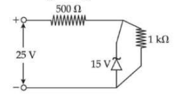
A Zener diode is used in a voltage regulator circuit as shown below. Its breakdown voltage is 15 V. What is the current flowing through the Zener diode?
Choose the correct experimental circuit arrangement for studying V-I characteristics of a p-n junction diode in forward bias: