MOSFET Switching Characteristics Influencing Factors
The speed at which a power MOSFET turns on and off, known as its switching characteristics, is critical for efficient operation in power electronic circuits like inverters and converters. Several factors influence this switching speed. Let's analyze the key elements:
Understanding MOSFET Internal Capacitances
Power MOSFETs possess inherent parasitic capacitances due to their physical structure. The most significant ones influencing switching are:
- Gate-Source Capacitance ($C_{gs}$): This capacitance exists between the gate terminal and the source terminal.
- Drain-Source Capacitance ($C_{ds}$): This capacitance exists between the drain terminal and the source terminal. It's often less critical for switching speed itself but impacts voltage transitions.
- Gate-Drain Capacitance ($C_{gd}$): Also known as the Miller capacitance, this is the capacitance between the gate and drain terminals. It plays a significant role during switching because its effective capacitance increases due to the amplification effect during the transition (Miller effect).
To turn the MOSFET ON, the gate voltage must rise above the threshold voltage ($V_{th}$). This requires charging $C_{gs}$ and $C_{gd}$. To turn the MOSFET OFF, the gate voltage must fall below $V_{th}$, requiring the discharge of these capacitances.
Role of Gate Drive Circuit Impedance
The gate drive circuit provides the necessary voltage and current to control the MOSFET's gate. The characteristics of this drive circuit are crucial:
- Gate Drive Impedance: This refers to the effective resistance and inductance presented by the gate driver circuit to the MOSFET's gate terminal.
- Current Delivery: The drive circuit must supply the current needed to charge and discharge the internal MOSFET capacitances ($C_{gs}$ and $C_{gd}$) quickly. The rate of charging/discharging determines the switching times (rise time, fall time).
- Relationship: A lower internal impedance of the gate drive circuit allows for a higher peak current to be delivered to the gate. This higher current can charge or discharge the capacitances more rapidly, resulting in faster switching transitions (shorter rise and fall times). Conversely, a high impedance drive circuit will lead to slower charging/discharging and thus slower switching.
- Mathematical Insight: While a simplified model might show time constant $\tau = R_{drive} \times C_{gate}$, where $C_{gate}$ represents the relevant input capacitance ($C_{gs} + C_{gd}$ effectively), the impedance ($R_{drive}$) directly impacts the speed.
Therefore, the combination of the MOSFET's internal capacitances and the impedance of the gate drive circuit dictates how quickly the gate voltage can change, thereby controlling the switching speed.
Why Other Factors Are Less Critical
While other parameters can have some influence, they are generally secondary compared to the internal capacitances and gate drive impedance:
- External Impedance/Capacitance: External components primarily connect the gate driver to the MOSFET gate. While improper selection can degrade performance, the fundamental switching speed is limited by the internal device capacitances and the driver's capability (impedance). External source or drain impedances don't directly control the gate charge/discharge rate.
- Source/Drain Terminals: The source terminal is the common reference, and its impedance primarily affects source inductance issues. The drain terminal impedance is related more to the load connected and the voltage characteristics rather than the gate switching speed.
In summary, the internal capacitances ($C_{gs}$, $C_{gd}$) of the MOSFET require charging and discharging, and the speed at which this happens is directly controlled by the current supplied by the gate drive circuit, which is limited by its internal impedance.
Important Questions from Power Semiconductor Diodes and Transistors
Which semiconductor power device, out of the following, is not a current triggered device?
Diacs are primarily used as:
Which of the following circuit is used to obtain pulse gate triggering?
The figure shows a straight-line approximation for the forward characteristics of a power diode. A continuous on-state current of 15 A is flowing through the diode.
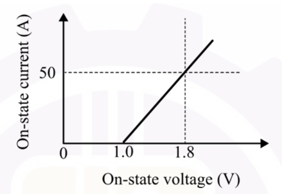
What is the power loss in the diode?
For a system with $G(S)=\frac{k}{S(S+1)(S+2)}$, $H(S)=1$. Determine the brake away point.