The O in a MOSFET stands for _______ layer which provides _______ to the device.
Oxide, high input impedance
Understanding the MOSFET Acronym
The acronym MOSFET stands for Metal-Oxide-Semiconductor Field-Effect Transistor. This name itself provides significant insight into the device's structure and fundamental operating principles. Each part of the acronym, including the "O", refers to a critical component or characteristic that defines this widely used semiconductor device.
The "O" in MOSFET: Oxide Layer Explained
In the context of a MOSFET, the letter O specifically represents the Oxide layer. This layer is an essential insulating material positioned strategically within the transistor's structure.
- The oxide layer typically consists of silicon dioxide (\(\text{SiO}_2\)) when silicon is the chosen semiconductor material for the device.
- It serves as an electrical insulator, effectively separating the metal gate terminal from the semiconductor substrate, where the channel forms.
- This insulating barrier is crucial for controlling the current flow through the device by applying a voltage to the gate.
Oxide Layer's Contribution: High Input Impedance
The primary function of the insulating oxide layer is to provide a characteristic feature of the MOSFET device: high input impedance. This property is vital for many electronic circuit applications.
- Due to the insulating nature of the oxide layer, it presents an extremely high resistance to any current attempting to flow into the gate terminal from the input signal source.
- Consequently, the gate of a MOSFET draws only a negligible amount of current, making it appear as a very high impedance load to the signal source.
- This high input impedance is a major advantage of MOSFETs over other types of transistors, such as Bipolar Junction Transistors (BJTs), which are current-controlled and generally exhibit lower input impedance.
- The ability to draw very little current from the input signal source makes MOSFETs ideal for applications requiring minimal signal loading, such as in the input stages of amplifiers, buffer circuits, and various digital logic gates.
Therefore, the O in MOSFET signifies the Oxide layer, which is instrumental in providing the device with its characteristic high input impedance.
Important Questions from MOSFET
Which industry does aluminium smelting belong to?
In an N-channel MOSFET, the drain current ID increases as _______.
Consider an ideal long channel nMOSFET (enhancement-mode) with gate length 10 µm and width 100 µm. The product of electron mobility (µn) and oxide capacitance per unit area (COX) is µn COX = 1 mA/V2 . The threshold voltage of the transistor is 1 V. For a gate-to-source voltage VGS = [2 − sin (2t)] V and drain-to-source voltage VDS = 1 V (substrate connected to the source), the maximum value of the drain-to-source current is ________.
- A power MOSFET is a ___________, __________ controlled and ___________ carrier device.
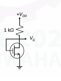
An n-channel MOSFET is connected as shown in the Figure.
Assume $V_{TH} = 1\text{ V}$, $V_{DD} = 5\text{ V}$, and $\mu C_{ox}\left(\frac{W}{L}\right) = 2\text{ mA V}^{-2}$ and neglect channel length modulation effects.
The gate voltage ($V_G$) of the n-channel MOSFET (in Volt) is __.
(rounded off to two decimal places)