When a diode is switching from conducting state to blocking state, it has stored charge which needs to be discharged before, it blocks reverse current, this time required is known as _______.
Reverse Recovery Time
Understanding Diode Switching Time: Reverse Recovery
When a semiconductor diode is operating in the forward-biased state, charge carriers (electrons and holes) flow across the p-n junction, allowing current to conduct easily. However, when the external voltage is suddenly reversed, attempting to switch the diode into a blocking state (reverse bias), the diode does not immediately stop conducting.
This is because there is a significant amount of "stored charge" within the semiconductor material, particularly in the depletion region and the neutral regions near the junction. These excess minority carriers need to be removed or recombine before the diode can effectively block the reverse voltage and current. The time it takes for this stored charge to dissipate, allowing the reverse current to drop to a small leakage value, is a crucial parameter related to the diode's switching speed.
Let's look at the options provided in the context of diode switching characteristics:
- Forward Recovery Time: This refers to the time it takes for the diode's forward voltage to reach its steady-state value after switching from reverse bias to forward bias. It's related to the charge build-up needed for forward conduction, not the removal of charge during turn-off.
- Reverse Recovery Time: This is the time required for the current through the diode to fall from its forward value to a specified low value (usually a percentage of the peak reverse current or leakage level) when switching from forward bias to reverse bias. This time is dominated by the need to discharge the stored minority carriers. The question specifically mentions the need to discharge stored charge before blocking reverse current, which precisely describes this phenomenon.
- Forward Conduction Time: This isn't a standard switching parameter. It simply refers to the duration for which the diode is conducting in the forward direction in a given circuit cycle.
- Reverse Conduction Time: This term is not a standard switching characteristic in this context. Ideally, a reverse-biased diode blocks current. Any reverse conduction would typically be associated with breakdown voltage being exceeded or leakage current, not the dynamic switching process from forward to reverse bias under normal operating conditions.
Therefore, the time required for a diode to switch from a conducting state to a blocking state, involving the discharge of stored charge before it blocks reverse current, is known as the Reverse Recovery Time.
Diode Reverse Recovery Time Explained
When the voltage across a diode is switched from forward to reverse:
- The current does not instantly drop to zero.
- For a short period, reverse current flows because of the stored minority carriers.
- This reverse current might even reach a peak value before dropping off.
- The time from the instant the voltage is reversed to the point where the reverse current drops to a negligible level is the reverse recovery time (\(t_{rr}\)).
- High-speed switching diodes and Schottky diodes are designed to minimize this reverse recovery time by reducing stored charge.
Revision Table: Diode Switching Times
| Parameter | Description | Switching Direction |
|---|---|---|
| Forward Recovery Time (\(t_{fr}\)) | Time for forward voltage to stabilize after switching from reverse to forward bias. | Reverse to Forward |
| Reverse Recovery Time (\(t_{rr}\)) | Time for current to drop to negligible reverse value after switching from forward to reverse bias, due to stored charge. | Forward to Reverse |
Additional Information on Diode Switching Characteristics
Diode switching speed is a critical factor in high-frequency circuits and power electronics. The stored charge effect limits how quickly a standard p-n junction diode can turn off. During the reverse recovery process, a significant reverse current flows for a brief period, which can lead to power dissipation and voltage spikes in the circuit. This reverse current is often called the "reverse recovery current". Minimizing reverse recovery time is essential for efficient high-speed switching applications.
Important Questions from Characteristics of Power Diodes
The barrier voltage for germanium is _________ at 25°C.
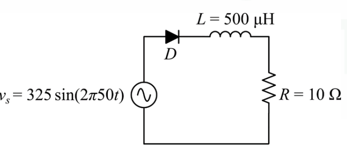
Consider the circuit shown. Assume that the diode $D$ is ideal. The supply voltage $v_s = 325 \sin(2\pi 50t) \text{ V}$, $L = 500 \mu H$, and $R = 10 \text{ }\Omega$. The peak diode current (in amperes) is ______________
(Round off to one decimal place)